
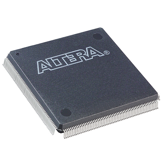
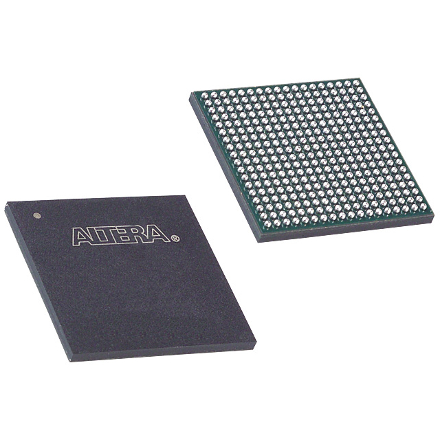
EP1C20F324C7
| Part Description |
Cyclone® Field Programmable Gate Array (FPGA) IC 233 294912 20060 324-BGA |
|---|---|
| Quantity | 1,125 Available (as of June 14, 2026) |

| Product Category | Field Programmable Gate Array (FPGA) |
|---|---|
| Manufacturer | Intel |
| Manufacturing Status | Obsolete |
| Manufacturer Standard Lead Time | Contact Us |
| Datasheet |
Specifications & Environmental
| Device Package | 324-FBGA (19x19) | Grade | Commercial | Operating Temperature | 0°C – 85°C | ||
|---|---|---|---|---|---|---|---|
| Package / Case | 324-BGA | Number of I/O | 233 | Voltage | 1.425 V - 1.575 V | ||
| Mounting Method | Surface Mount | RoHS Compliance | RoHS non-compliant | REACH Compliance | REACH Unknown | ||
| Moisture Sensitivity Level | 3 (168 Hours) | Number of LABs/CLBs | 2006 | Number of Logic Elements/Cells | 20060 | ||
| Number of Gates | N/A | ECCN | 3A991D | HTS Code | 8542.39.0001 | ||
| Qualification | N/A | Total RAM Bits | 294912 |
Overview of EP1C20F324C7 – Cyclone® Field Programmable Gate Array (FPGA) IC 233 294912 20060 324-BGA
The EP1C20F324C7 is an Intel Cyclone® family FPGA device delivering 20,060 logic elements and 294,912 bits of on-chip RAM. It is built on the Cyclone architecture described in the device handbook and is optimized for data-path applications and system interfacing where a balance of density, I/O capability, and cost-effective integration is required.
Designed for commercial-grade applications, this surface-mount 324-ball FBGA package supports a broad set of I/O standards and clocking resources, making it suitable for designs requiring flexible memory interfaces, high-speed I/O, and integrated clock management while operating within a 1.425 V to 1.575 V supply window and 0 °C to 85 °C temperature range.
Key Features
- Core Logic 20,060 logic elements provide substantial combinational and sequential logic capacity for mid-density FPGA designs.
- Embedded Memory 294,912 bits of on-chip RAM (approximately 0.295 Mbits) for data buffering, FIFOs, and memory-intensive datapath functions.
- I/O Capacity & Standards 233 I/O pins and family-level support for LVTTL, LVCMOS, SSTL-2/SSTL-3 and high-speed LVDS enable interfacing with a wide variety of peripherals and external devices.
- Clocking & Timing Family architecture provides up to two PLLs and multiple global clock resources to support clock multiplication, phase shifting, and synchronized multi-clock designs.
- Memory Interfaces Cyclone family support includes dedicated DDR and SDR memory interface capability for DDR SDRAM, FCRAM, and SDR SDRAM connectivity.
- Package & Mounting 324-ball FineLine BGA (324-FBGA, 19 × 19) in a surface-mount package for compact board integration and reliable thermal/power distribution.
- Power & Operating Range Device supply range 1.425 V to 1.575 V and commercial operating temperature 0 °C to 85 °C.
- Compliance RoHS-compliant construction for regulatory and manufacturing considerations.
Typical Applications
- Data-path processing Use the device's 20,060 logic elements and embedded RAM for packet processing, signal conditioning, or custom datapath blocks.
- Memory controller and buffering Implement DDR SDRAM or SDRAM interface logic and on-board buffering using the device’s RAM and dedicated memory interface capability.
- High-speed serial and parallel I/O Support LVDS and a variety of I/O standards for camera interfaces, display bridging, and high-speed link aggregation.
- Peripheral and bus bridging Create custom PCI/bridge logic or peripheral adapters using abundant I/O and clocking resources.
Unique Advantages
- Substantial logic density: 20,060 logic elements enable complex state machines, DSP blocks, and control logic within a single device, reducing system BOM.
- On-chip memory for efficient buffering: Nearly 295kbits of embedded RAM supports deep FIFOs and local scratch memory without external RAM overhead.
- Flexible I/O and interface support: 233 I/O pins and family-level support for multiple standards let you connect diverse peripherals without extra interface chips.
- Integrated clocking resources: Up to two PLLs and multiple global clocks simplify timing architectures for multi-rate systems and synchronous designs.
- Compact BGA packaging: The 324-FBGA (19 × 19) package offers a space-efficient implementation for high-density board layouts.
- Regulatory readiness: RoHS compliance supports modern manufacturing and environmental requirements.
Why Choose EP1C20F324C7?
The EP1C20F324C7 combines a mid-to-high logic capacity with ample on-chip memory and extensive I/O, making it a practical choice for commercial applications that need balanced performance, interface flexibility, and compact packaging. Its Cyclone family architecture provides the clocking and memory interface features designers rely on for data-path and bridging applications.
This device is well suited for engineering teams implementing mid-density FPGA solutions who require predictable supply voltage and operating-temperature boundaries and who value the Cyclone architecture's integration of PLLs, global clocks, and embedded RAM for robust system design.
Request a quote or submit your design requirements to receive pricing and availability information for the EP1C20F324C7.


Date Founded: 1968
Headquarters: Santa Clara, California, USA
Employees: 130,000+
Revenue: $54.23 Billion
Certifications and Memberships: ISO9001:2015, ISO14001:2015, ISO17025:2017, ISO27001:2022, ISO45001:2018, ISO50001:2018


