
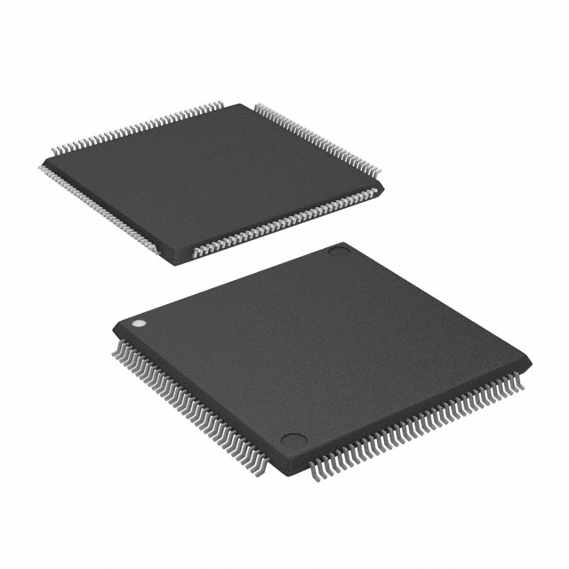
EP1C3T144C8N
| Part Description |
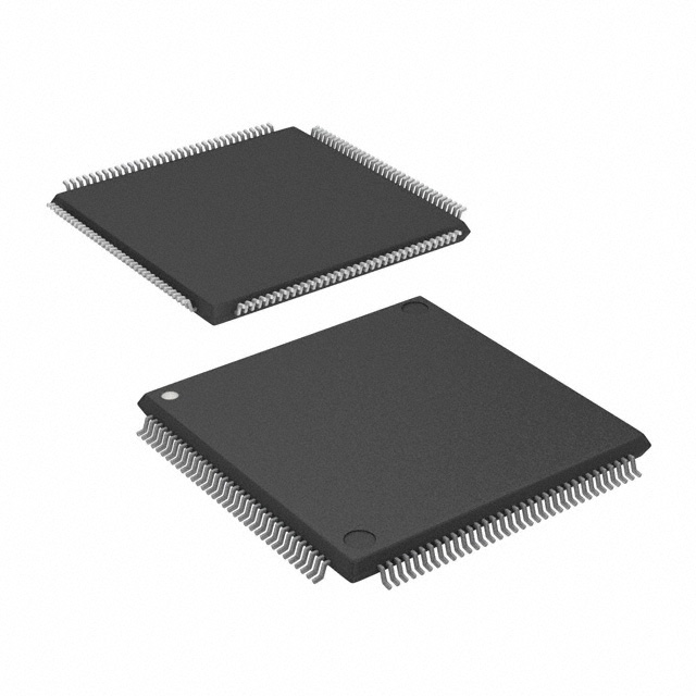
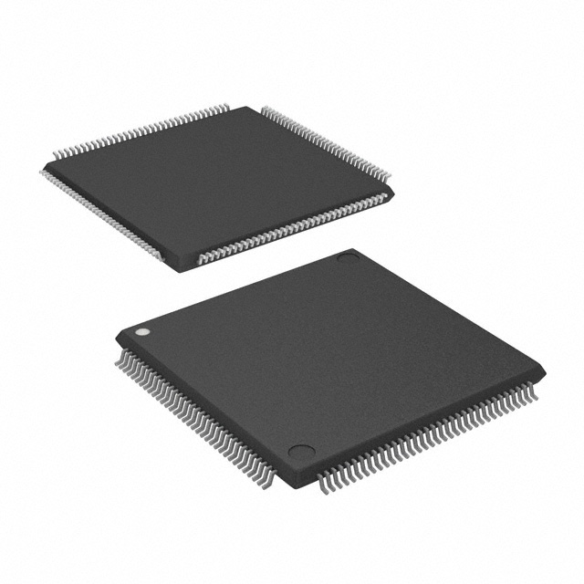
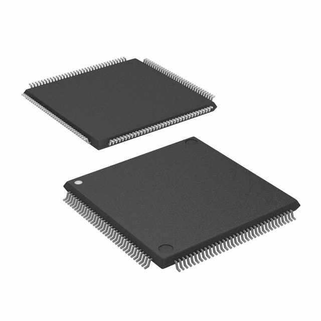
Cyclone® Field Programmable Gate Array (FPGA) IC 104 59904 2910 144-LQFP |
|---|---|
| Quantity | 1,060 Available (as of October 7, 2026) |
| Product Category | Field Programmable Gate Array (FPGA) |
|---|---|
| Manufacturer | Intel |
| Manufacturing Status | Obsolete |
| Manufacturer Standard Lead Time | Contact Us |
| Datasheet |
Specifications & Environmental
| Device Package | 144-TQFP (20x20) | Grade | Commercial | Operating Temperature | 0°C – 85°C | ||
|---|---|---|---|---|---|---|---|
| Package / Case | 144-LQFP | Number of I/O | 104 | Voltage | 1.425 V - 1.575 V | ||
| Mounting Method | Surface Mount | RoHS Compliance | Unknown | REACH Compliance | REACH Unknown | ||
| Moisture Sensitivity Level | 3 (168 Hours) | Number of LABs/CLBs | 291 | Number of Logic Elements/Cells | 2910 | ||
| Number of Gates | N/A | ECCN | 3A991D | HTS Code | 8542.39.0001 | ||
| Qualification | N/A | Total RAM Bits | 59904 |
Overview of EP1C3T144C8N – Cyclone® Field Programmable Gate Array (FPGA) IC 104 59904 2910 144-LQFP
The EP1C3T144C8N is a Cyclone® family Field Programmable Gate Array (FPGA) delivered in a 144-pin quad flat package. Built around a Cyclone architecture, this commercial-grade device provides a compact, reprogrammable logic platform with a balance of logic density, on-chip memory, and I/O resources for cost-sensitive data-path and control applications.
With 2,910 logic elements, 291 logic array blocks (LABs), and 59,904 bits of embedded RAM, the device targets system designers requiring flexible hardware acceleration, custom peripheral interfacing, and memory-attached logic in a small form factor. The device operates on a core supply between 1.425 V and 1.575 V and is rated for commercial temperature operation from 0 °C to 85 °C.
Key Features
- Core Logic — 2,910 logic elements organized across 291 LABs, providing reprogrammable combinational and sequential logic resources for control, glue-logic, and custom datapath functions.
- Embedded Memory — 59,904 total RAM bits of on-chip memory (approximately 0.06 Mbits) for FIFOs, small buffers, and state storage inside the FPGA fabric.
- I/O Resources — Up to 104 user I/O pins (including global clock pins) to interface with peripherals, memory, and external ASICs.
- Clocking — Device-level clocking resources consistent with the Cyclone family (EP1C3 device class), including dedicated clock networks to support synchronous designs.
- Power — Core voltage range of 1.425 V to 1.575 V, enabling predictable power provisioning for board-level designs.
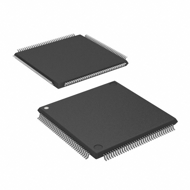
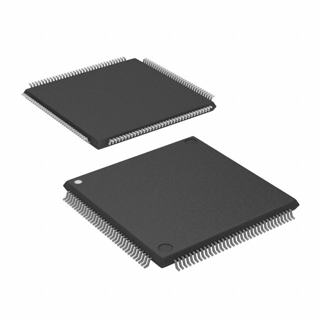
- Package — Surface-mount 144-pin LQFP package (supplier device package listed as 144-TQFP, 20×20 mm), designed for compact PCB layouts.
- Temperature & Grade — Commercial grade operation from 0 °C to 85 °C, suitable for consumer and general-purpose embedded applications.
- Compliance — RoHS-compliant manufacturing and materials.
Typical Applications
- Data-path Acceleration — Implement custom arithmetic, packet processing, or protocol handling logic where moderate logic density and local RAM are required.
- Memory Interface Glue Logic — Serve as an interface or controller for external memory subsystems, leveraging embedded RAM and dedicated clocking resources.
- Peripheral Bridging and Integration — Aggregate and translate signals between various peripherals and host processors using the device’s 104 I/O pins.
- Control and Monitoring — Implement motor control state machines, sensor aggregation, or real-time control logic in compact commercial systems.
Unique Advantages
- Balanced Logic and Memory: 2,910 LEs combined with nearly 60k bits of embedded RAM enable mixed control and buffering tasks without external memory for many use cases.
- Compact, PCB-friendly Package: 144-pin LQFP/TQFP packaging provides a small board footprint while exposing up to 104 usable I/O pins for flexible system connectivity.
- Deterministic Power Envelope: Narrow core supply window (1.425–1.575 V) simplifies power-supply selection and board-level power distribution planning.
- Commercial Temperature Range: 0 °C to 85 °C rating matches typical consumer and general embedded deployments where commercial-grade components are required.
- RoHS-compliant: Conforms to RoHS environmental requirements for regulated materials.
Why Choose EP1C3T144C8N?
The EP1C3T144C8N delivers a practical combination of reprogrammable logic, on-chip memory, and I/O density in a compact 144-pin package, making it well suited for designers building cost-conscious data-path, control, and peripheral integration solutions. Its Cyclone family architecture provides established FPGA capabilities—sufficient logic resources and embedded RAM—while maintaining predictable power and thermal behavior for commercial embedded systems.
This device is a fit for customers who need a scalable, reprogrammable building block for prototypes, production devices, or mid-volume products where compact packaging, moderate logic density, and compliance to RoHS are important selection criteria.
Request a quote or submit an inquiry to obtain pricing, availability, and lead-time information for EP1C3T144C8N and to discuss how this FPGA can be integrated into your next design.





















Date Founded: 1968
Headquarters: Santa Clara, California, USA
Employees: 130,000+
Revenue: $54.23 Billion
Certifications and Memberships: ISO9001:2015, ISO14001:2015, ISO17025:2017, ISO27001:2022, ISO45001:2018, ISO50001:2018


