
EP1C3T144I7
| Part Description |
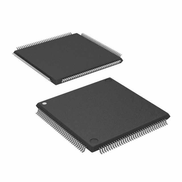
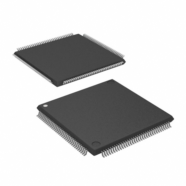
Cyclone® Field Programmable Gate Array (FPGA) IC 104 59904 2910 144-LQFP |
|---|---|
| Quantity | 499 Available (as of October 7, 2026) |
| Product Category | Field Programmable Gate Array (FPGA) |
|---|---|
| Manufacturer | Intel |
| Manufacturing Status | Obsolete |
| Manufacturer Standard Lead Time | Contact Us |
| Datasheet |
Specifications & Environmental
| Device Package | 144-TQFP (20x20) | Grade | Industrial | Operating Temperature | -40°C – 100°C | ||
|---|---|---|---|---|---|---|---|
| Package / Case | 144-LQFP | Number of I/O | 104 | Voltage | 1.425 V - 1.575 V | ||
| Mounting Method | Surface Mount | RoHS Compliance | RoHS non-compliant | REACH Compliance | REACH Unknown | ||
| Moisture Sensitivity Level | 3 (168 Hours) | Number of LABs/CLBs | 291 | Number of Logic Elements/Cells | 2910 | ||
| Number of Gates | N/A | ECCN | 3A991D | HTS Code | 8542.39.0001 | ||
| Qualification | N/A | Total RAM Bits | 59904 |
Overview of EP1C3T144I7 – Cyclone® Field Programmable Gate Array (FPGA) IC 104 59904 2910 144-LQFP
The EP1C3T144I7 is a Cyclone® FPGA device from Intel designed for cost-sensitive, data-path and interface applications. It implements the Cyclone family architecture built on a 1.5-V, 0.13-µm, all-layer copper SRAM process and provides a compact, industrial-grade programmable logic option.
With 2,910 logic elements, approximately 59,904 bits of embedded RAM, and 104 user I/O pins in a 144-pin LQFP surface-mount package, this device targets embedded systems, memory-interface logic, and I/O-centric designs that require low-voltage operation and industrial temperature capability.
Key Features
- Core Architecture Cyclone family SRAM-based FPGA architecture implemented in a 1.5-V, 0.13-µm process, delivering 2,910 logic elements suitable for moderate-density digital designs.
- On-chip Memory Approximately 59,904 bits of embedded RAM organized as M4K blocks (EP1C3 device includes 13 M4K blocks) for buffering, FIFOs, and small data stores.
- I/O and Interface Support 104 user I/O pins (includes global clock pins) with support in the Cyclone family for common I/O standards such as LVTTL, LVCMOS, SSTL-2, SSTL-3 and LVDS, enabling flexible interfacing to memory and ASSP/ASIC devices.
- Clocking Resources Includes one PLL on the EP1C3 device and the Cyclone family provides multiple global clock resources and clock routing to support synchronous designs.
- Power and Supply Nominal low-voltage operation with a recommended voltage supply range of 1.425 V to 1.575 V, matching low-voltage system rails.
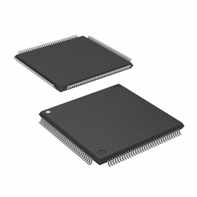
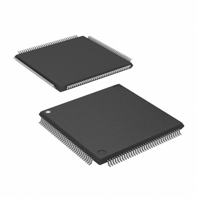
- Package and Mounting 144-pin LQFP surface-mount package; supplier device package also listed as 144-TQFP (20×20). Ideal for compact PCB layouts that require a standard flat-pack surface-mount footprint.
- Industrial Temperature Grade Rated for operation from −40 °C to 100 °C, suitable for industrial environments.
- Regulatory RoHS compliant.
Typical Applications
- Data-path Processing Implement finite state machines, bit-level processing, and moderate-density combinational/sequential logic for throughput-focused applications.
- Memory Interface Logic Use the device’s DDR/SDRAM interface support and on-chip RAM for buffering and protocol translation between memory and host logic.
- Peripheral and Bus Bridging Serve as an interface bridge between ASSP/ASIC components and system buses, leveraging flexible I/O standards and available clocking resources.
- Embedded Control and Sensor Systems Integrate control logic, I/O aggregation, and lightweight processing for industrial embedded systems operating across a wide temperature range.
Unique Advantages
- Compact, surface-mount package: 144-pin LQFP/TQFP footprint provides a space-efficient solution for board-level integration while retaining ample I/O.
- Industrial operating range: Rated from −40 °C to 100 °C to meet industrial deployment requirements.
- Low-voltage FPGA core: Operates within a 1.425 V to 1.575 V supply window compatible with low-voltage system designs.
- Integrated memory resources: Approximately 59,904 bits of on-chip RAM (13 M4K blocks on EP1C3) reduce external memory requirements for small buffers and FIFOs.
- Flexible I/O standards: Cyclone family support for LVTTL, LVCMOS, SSTL, and LVDS helps simplify interfacing to a variety of peripherals and memory devices.
- Tool and IP ecosystem: Cyclone devices are supported by Quartus II design flows and Altera MegaCore/AMPP megafunctions for design productivity and IP reuse.
Why Choose EP1C3T144I7?
The EP1C3T144I7 positions itself as a practical, industrial-grade FPGA for designers needing a balance of moderate logic capacity, embedded memory, and flexible I/O in a compact surface-mount package. Its low-voltage core, single on-chip PLL, and Cyclone family architecture make it a good fit for data-path tasks, memory interfacing and I/O aggregation in industrial and embedded systems.
Designed for teams that value predictable integration and toolchain support, the EP1C3T144I7 benefits from Cyclone family design resources and IP, enabling scalable migration paths within the Cyclone lineup and streamlined implementation using established development tools.
If you would like pricing, availability, or to request a quote for the EP1C3T144I7, please submit a quote request or contact our sales channel for further assistance.





















Date Founded: 1968
Headquarters: Santa Clara, California, USA
Employees: 130,000+
Revenue: $54.23 Billion
Certifications and Memberships: ISO9001:2015, ISO14001:2015, ISO17025:2017, ISO27001:2022, ISO45001:2018, ISO50001:2018


