
EP1K100FC256-1N
| Part Description |
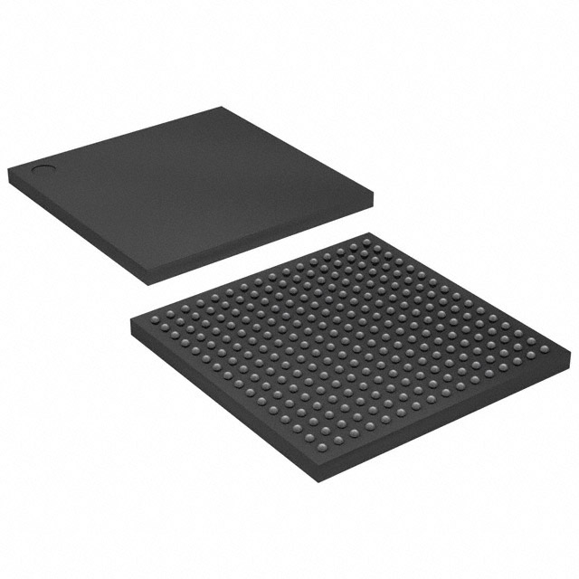
ACEX-1K® Field Programmable Gate Array (FPGA) IC 186 49152 4992 256-BGA |
|---|---|
| Quantity | 858 Available (as of June 15, 2026) |
| Product Category | Field Programmable Gate Array (FPGA) |
|---|---|
| Manufacturer | Intel |
| Manufacturing Status | Obsolete |
| Manufacturer Standard Lead Time | Contact Us |
| Datasheet |
Specifications & Environmental
| Device Package | 256-FBGA (17x17) | Grade | Commercial | Operating Temperature | 0°C – 70°C | ||
|---|---|---|---|---|---|---|---|
| Package / Case | 256-BGA | Number of I/O | 186 | Voltage | 2.375 V - 2.625 V | ||
| Mounting Method | Surface Mount | RoHS Compliance | Unknown | REACH Compliance | REACH Unaffected | ||
| Moisture Sensitivity Level | 3 (168 Hours) | Number of LABs/CLBs | 624 | Number of Logic Elements/Cells | 4992 | ||
| Number of Gates | 257000 | ECCN | 3A991D | HTS Code | 8542.39.0001 | ||
| Qualification | N/A | Total RAM Bits | 49152 |
Overview of EP1K100FC256-1N – ACEX-1K® Field Programmable Gate Array (FPGA), 256-BGA
The EP1K100FC256-1N is an Intel ACEX-1K series field programmable gate array (FPGA) designed for mid- to high-density programmable logic integration. Built as a cost-efficient programmable logic device (PLD) with embedded array blocks, it is suited for system-on-a-programmable-chip (SOPC) integration, memory-intensive megafunctions, and communication-focused designs.
This device combines a sizable logic capacity with on-chip RAM and flexible I/O capabilities, delivering a platform for designers who need integrated logic, embedded memory, and multi-voltage I/O in a compact 256-ball fine-pitch BGA package.
Key Features
- Core logic capacity — 4,992 logic elements (LEs) providing a maximum system gates figure of 257,000 to support complex combinational and sequential logic implementations.
- Embedded memory — 49,152 bits of on-chip RAM implemented across embedded array blocks (EABs), enabling dual-port memory configurations and megafunction support for efficient on-chip data storage.
- I/O and MultiVolt support — 186 user I/O pins with MultiVolt I/O capability that can interface with 2.5 V, 3.3 V, or 5.0 V devices; device operates with an internal supply in the 2.375 V to 2.625 V range (nominal 2.5 V).
- Package and mounting — 256-ball fine-pitch BGA (256-FBGA, 17×17) surface-mount package that balances routing density and board-area efficiency for compact designs.
- Clocking and dedicated routing — Built-in low-skew clock distribution trees, multiple global clock and clear signals, dedicated carry and cascade chains, and FastTrack interconnect for predictable routing and arithmetic performance.
- Configuration and test — In-circuit reconfigurability via external configuration devices, intelligent controllers, or JTAG; built-in JTAG boundary-scan test (IEEE 1149.1) available without consuming device logic.
- Commercial temperature and grade — Commercial-grade device rated for operation from 0 °C to 70 °C.
- Design and tool support — Series-level software design support and automatic place-and-route tools are provided for common development environments and EDA interfaces.
Typical Applications
- System-on-a-programmable-chip (SOPC) — Integrate custom logic, controllers, and memory-intensive megafunctions into a single device for compact system designs.
- Communications equipment — Implement protocol handling, buffering and data-path logic for high-performance communications applications.
- PCI and bus-interface logic — Support for PCI Local Bus Specification (as provided for the series) enables use in systems requiring compliant bus-interface logic at standard voltages and bus speeds.
- Embedded memory functions — Use the device’s 49,152 bits of on-chip RAM and dual-port EAB capability for FIFOs, small data buffers, and other memory-heavy functions.
Unique Advantages
- Highly integrated logic and memory — Combines 4,992 logic elements with 49,152 bits of embedded RAM to reduce external memory needs and simplify board design.
- Flexible I/O interfacing — MultiVolt I/O and programmable pin features (tri-state control, open-drain option, selectable clamp to VCCIO) allow straightforward interfacing with a range of peripheral voltage domains.
- In-system configurability and test — JTAG boundary-scan and in-circuit reconfigurability support rapid development cycles, field updates, and board-level test strategies without consuming device logic.
- Predictable performance routing — Dedicated carry and cascade chains along with low-skew clock trees and FastTrack interconnect reduce timing uncertainty for arithmetic and high-fan-in logic.
- Compact, surface-mount packaging — 256-FBGA (17×17) package provides a compact solution for space-constrained boards while supporting a substantial I/O count.
Why Choose EP1K100FC256-1N?
The EP1K100FC256-1N positions itself as a commercially graded, mid- to high-density FPGA option within the ACEX-1K family, offering a balanced combination of logic capacity, embedded RAM, and MultiVolt I/O flexibility. Its integrated configuration and test features, along with dedicated routing resources, make it suitable for designers targeting compact SOPC solutions and communication-oriented systems where on-chip memory and reliable clocking are important.
For teams and projects requiring a configurable, cost-efficient programmable logic device in a fine-pitch BGA package, the EP1K100FC256-1N delivers a verifiable set of capabilities that support scalable designs and established development tool flows.
Request a quote or submit a product inquiry today to evaluate EP1K100FC256-1N for your next design.


Date Founded: 1968
Headquarters: Santa Clara, California, USA
Employees: 130,000+
Revenue: $54.23 Billion
Certifications and Memberships: ISO9001:2015, ISO14001:2015, ISO17025:2017, ISO27001:2022, ISO45001:2018, ISO50001:2018


