
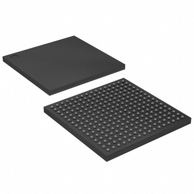
EP1K100FC256-2
| Part Description |
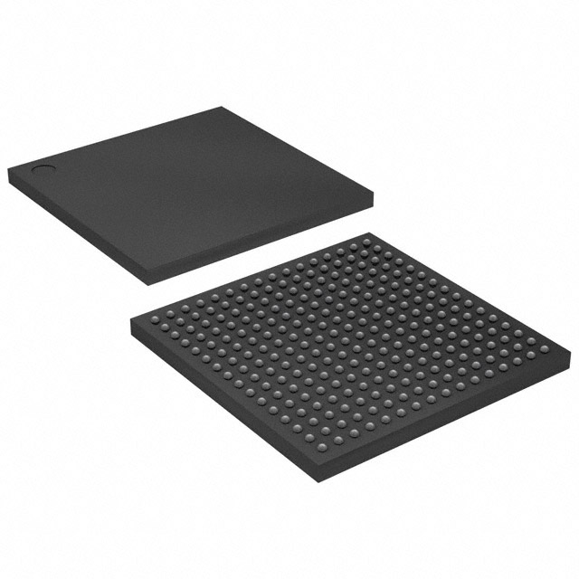
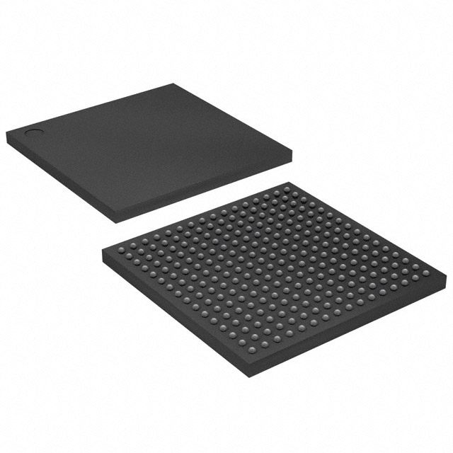
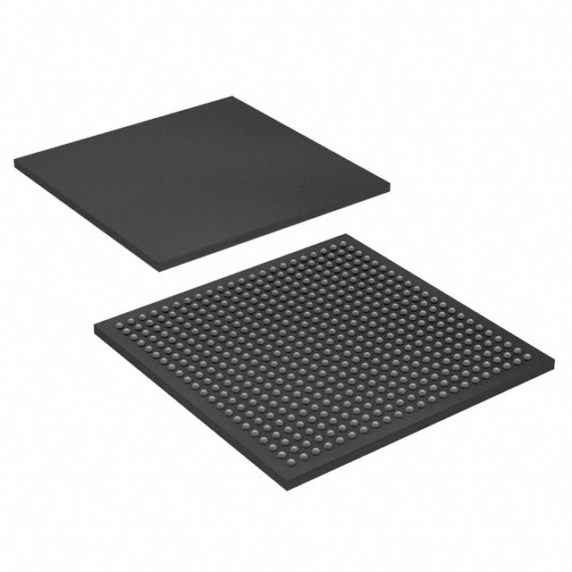
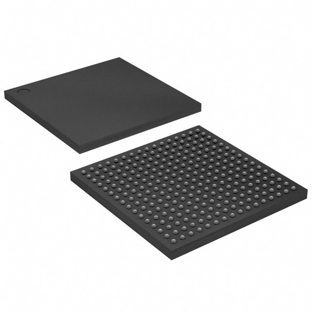
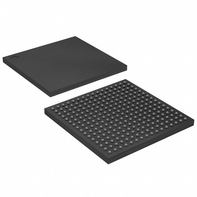
ACEX-1K® Field Programmable Gate Array (FPGA) IC 186 49152 4992 256-BGA |
|---|---|
| Quantity | 1,442 Available (as of October 8, 2026) |
| Product Category | Field Programmable Gate Array (FPGA) |
|---|---|
| Manufacturer | Intel |
| Manufacturing Status | Obsolete |
| Manufacturer Standard Lead Time | Contact Us |
| Datasheet |
Specifications & Environmental
| Device Package | 256-FBGA (17x17) | Grade | Commercial | Operating Temperature | 0°C – 70°C | ||
|---|---|---|---|---|---|---|---|
| Package / Case | 256-BGA | Number of I/O | 186 | Voltage | 2.375 V - 2.625 V | ||
| Mounting Method | Surface Mount | RoHS Compliance | RoHS non-compliant | REACH Compliance | REACH Unaffected | ||
| Moisture Sensitivity Level | 3 (168 Hours) | Number of LABs/CLBs | 624 | Number of Logic Elements/Cells | 4992 | ||
| Number of Gates | 257000 | ECCN | 3A991D | HTS Code | 8542.39.0001 | ||
| Qualification | N/A | Total RAM Bits | 49152 |
Overview of EP1K100FC256-2 – ACEX‑1K® Field Programmable Gate Array (FPGA), 256‑BGA
The EP1K100FC256-2 is an ACEX‑1K family programmable logic device (FPGA) from Intel, designed for system-on-a-programmable-chip integration. It combines a logic array with embedded array blocks (EABs) to support megafunctions, on-chip RAM, and general logic functions for communications, embedded control, and low‑cost high‑volume applications.
With 4,992 logic elements, 49,152 bits of embedded RAM and a 256‑ball FineLine BGA package, this commercial‑grade device targets designs that require moderate logic density, flexible I/O, and in‑circuit reconfigurability within a 0 °C to 70 °C operating range.
Key Features
- Logic Capacity — 4,992 logic elements and 257,000 maximum system gates provide substantial programmable logic for mid‑range FPGA designs.
- Embedded Memory (EABs) — Up to 49,152 bits of on‑chip RAM (4,096 bits per embedded array block) with dual‑port capability and up to 16‑bit width per block for efficient megafunction and buffer implementation.
- I/O and Voltage Flexibility — 186 user I/O pins with MultiVolt capability to interface with different voltage domains; device operates with an internal supply in the 2.375 V to 2.625 V range.
- Package and Mounting — 256‑FBGA (17×17) FineLine BGA, surface‑mount package suitable for compact board designs.
- Configuration and Test — In‑circuit reconfigurability options and built‑in JTAG boundary‑scan (IEEE 1149.1) for programming and board‑level test without consuming device logic.
- Clock and Interconnect — Dedicated carry and cascade chains, built‑in low‑skew clock distribution, and options for reduced clock delay and skew to support high‑performance synchronous logic.
- Power and Reliability — Low power consumption characteristics and 100% functional testing at the device level; RoHS compliant.
- Commercial Temperature Range — Rated for operation from 0 °C to 70 °C for commercial applications.
Typical Applications
- Communications Equipment — Implement protocol logic, packet buffering, and custom data‑path functions using on‑chip RAM and dual‑port EABs.
- Embedded Control — Integrate control logic, interfaces, and timing functions for appliances, instrumentation, and consumer electronics.
- Prototyping and Development — Deploy as a reconfigurable platform for hardware validation, algorithm partitioning, and early system bring‑up.
- Peripheral and Interface Bridging — Use abundant I/O and voltage flexibility to bridge between different logic families and peripheral devices.
Unique Advantages
- Balanced Logic and Memory — 4,992 logic elements paired with 49,152 bits of embedded RAM lets designers implement both control and sizable on‑chip data storage without external memory.
- Flexible I/O Voltage Support — MultiVolt I/O capability enables direct interfacing to 2.5 V, 3.3 V, or 5.0 V domains, simplifying mixed‑voltage board designs.
- Compact, High‑Density Package — 256‑FBGA (17×17) package delivers a high pin count and compact footprint for space‑constrained boards.
- On‑board Reconfigurability and Test — In‑circuit reconfigurability plus JTAG boundary‑scan allow field updates and board‑level testing without consuming programmable logic.
- Deterministic Clocking and Arithmetic Support — Dedicated carry and cascade resources and low‑skew clock trees help implement high‑speed arithmetic and wide combinational functions efficiently.
- Compliance and Manufacturing Readiness — Commercial grade, surface‑mount BGA package and RoHS compliance support standard manufacturing flows.
Why Choose EP1K100FC256-2?
The EP1K100FC256-2 positions itself as a versatile, commercial‑grade FPGA for mid‑range designs that need a balanced mix of logic, embedded RAM, and flexible I/O in a compact BGA package. Its combination of 4,992 logic elements, 49,152 bits of on‑chip RAM, and dedicated interconnect resources makes it suitable for communications, embedded control, and prototyping tasks where in‑circuit reconfigurability and board‑level testability are important.
Choose this device when you require reliable, reconfigurable logic that integrates memory and dedicated arithmetic support while maintaining a compact footprint and compatibility with standard surface‑mount assembly processes.
Request a quote or submit a purchase inquiry to learn about availability and lead times for the EP1K100FC256-2.





















Date Founded: 1968
Headquarters: Santa Clara, California, USA
Employees: 130,000+
Revenue: $54.23 Billion
Certifications and Memberships: ISO9001:2015, ISO14001:2015, ISO17025:2017, ISO27001:2022, ISO45001:2018, ISO50001:2018


