
EP1K100FC484-2NGZ
| Part Description |
ACEX-1K® Field Programmable Gate Array (FPGA) IC 333 49152 4992 484-BBGA |
|---|---|
| Quantity | 1,110 Available (as of June 15, 2026) |

| Product Category | Field Programmable Gate Array (FPGA) |
|---|---|
| Manufacturer | Intel |
| Manufacturing Status | Obsolete |
| Manufacturer Standard Lead Time | Contact Us |
| Datasheet |
Specifications & Environmental
| Device Package | 484-FBGA (23x23) | Grade | Commercial | Operating Temperature | 0°C – 70°C | ||
|---|---|---|---|---|---|---|---|
| Package / Case | 484-BBGA | Number of I/O | 333 | Voltage | 2.375 V - 2.625 V | ||
| Mounting Method | Surface Mount | RoHS Compliance | Unknown | REACH Compliance | REACH Unknown | ||
| Moisture Sensitivity Level | 3 (168 Hours) | Number of LABs/CLBs | 624 | Number of Logic Elements/Cells | 4992 | ||
| Number of Gates | 257000 | ECCN | OBSOLETE | HTS Code | 0000.00.0000 | ||
| Qualification | N/A | Total RAM Bits | 49152 |
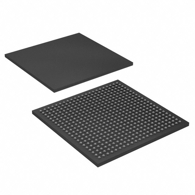
Overview of EP1K100FC484-2NGZ – ACEX-1K® FPGA, 4,992 logic elements, 49,152 RAM bits, 333 I/Os, 484-BBGA
The EP1K100FC484-2NGZ is an ACEX-1K family field programmable gate array (FPGA) optimized for system-on-a-programmable-chip integration. It combines a dense logic array with embedded array blocks (EABs) to implement memory-rich megafunctions and general-purpose logic for communications, embedded control and high-volume applications.
Designed for commercial-grade deployments, the device provides a combination of on-chip memory, a high I/O count and programmable I/O voltage support that streamlines integration of logic, memory and interface functions on a single surface-mount 484-BBGA package.
Key Features
- Core Logic 4,992 logic elements delivering up to 257,000 maximum system gates for compact implementation of combinational and sequential functions.
- Embedded Memory (EABs) Up to 49,152 total RAM bits (4,096 bits per EAB) and dual-port capability with up to 16-bit width per EAB to support memory-intensive functions and efficient megafunction implementation.
- I/O and Interfaces 333 user I/O pins with MultiVolt I/O capability (drive or be driven by 2.5 V, 3.3 V, or 5.0 V devices), enabling flexible interfacing to mixed-voltage systems.
- Configuration and Test Built-in JTAG boundary-scan (IEEE 1149.1) for in-system test and configuration; supports in-circuit reconfigurability via external configuration devices or JTAG port.
- Clocking and Performance Dedicated low-skew clock distribution trees, ClockLock and ClockBoost options, dedicated carry and cascade chains for arithmetic and high-fan-in logic—features that improve timing predictability for complex designs.
- Package and Mounting Surface-mount 484-BBGA package (supplier package: 484-FBGA, 23×23) suitable for compact board designs while providing high pin density.
- Power and Supply Operates with a 2.5 V internal supply and specified supply range of 2.375 V to 2.625 V for core power.
- Commercial Grade & Compliance Commercial operating grade with RoHS compliance; specified operating temperature range 0 °C to 70 °C.
Typical Applications
- Communications Equipment Implement packet processing, protocol bridging or custom interface logic using the device’s high I/O count and embedded RAM.
- Embedded Control and SoPC Integrate control engines, state machines and on-chip memory for compact system-on-programmable-chip solutions.
- Memory-Intensive Functions Use dual-port EABs and the available 49,152 RAM bits for FIFOs, buffering and lookup tables in data-path designs.
- PCI and Bus Interface Designs Employ family-level PCI Local Bus Specification support (for applicable device grades and configurations) to implement bus interface logic and local peripheral control.
Unique Advantages
- High integration density: Combine nearly 5,000 logic elements and substantial on-chip RAM to reduce external components and board footprint.
- Flexible voltage interfacing: MultiVolt I/O support enables direct interfacing to 2.5 V, 3.3 V or 5.0 V peripherals, simplifying mixed-voltage system design.
- Deterministic clocking: Built-in low-skew clock trees and clock-management options help achieve predictable timing for synchronous designs.
- On-board test and reconfiguration: JTAG boundary-scan and in-circuit reconfigurability streamline production test and field updates without consuming core logic.
- Compact, high-density packaging: 484-BBGA surface-mount package provides high pin count in a compact footprint for space-constrained PCBs.
- Regulatory and environmental readiness: RoHS compliant to meet current environmental requirements for commercial electronic products.
Why Choose EP1K100FC484-2NGZ?
The EP1K100FC484-2NGZ positions itself as a commercial-grade FPGA that balances logic density, embedded memory capacity and a high I/O count to address a wide range of communications and embedded system designs. Its MultiVolt I/O, deterministic clocking features and on-chip EAB resources help compress systems and reduce bill-of-materials costs.
This device is suited for engineers seeking a compact, reconfigurable platform with significant on-chip RAM and flexible interfacing options, backed by established ACEX-1K family architecture and tooling support referenced in the product datasheet.
Request a quote or submit an inquiry to get pricing and availability for the EP1K100FC484-2NGZ. Provide your quantity and lead-time needs for a tailored response.


Date Founded: 1968
Headquarters: Santa Clara, California, USA
Employees: 130,000+
Revenue: $54.23 Billion
Certifications and Memberships: ISO9001:2015, ISO14001:2015, ISO17025:2017, ISO27001:2022, ISO45001:2018, ISO50001:2018


