
EP1K100FC484-3N
| Part Description |
ACEX-1K® Field Programmable Gate Array (FPGA) IC 333 49152 4992 484-BBGA |
|---|---|
| Quantity | 1,342 Available (as of June 14, 2026) |

| Product Category | Field Programmable Gate Array (FPGA) |
|---|---|
| Manufacturer | Intel |
| Manufacturing Status | Obsolete |
| Manufacturer Standard Lead Time | Contact Us |
| Datasheet |
Specifications & Environmental
| Device Package | 484-FBGA (23x23) | Grade | Commercial | Operating Temperature | 0°C – 70°C | ||
|---|---|---|---|---|---|---|---|
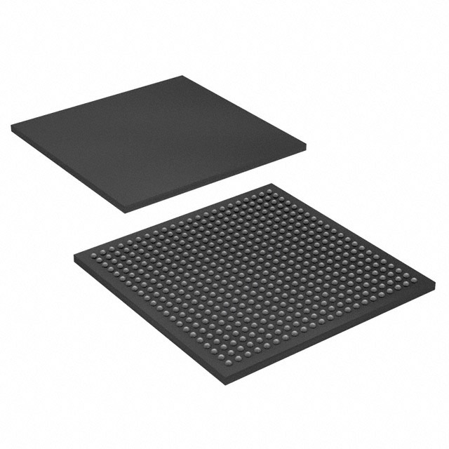
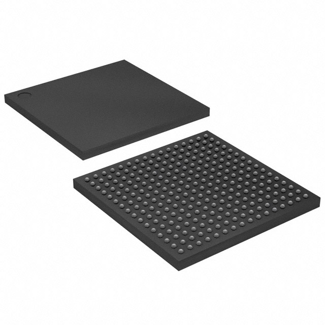
| Package / Case | 484-BBGA | Number of I/O | 333 | Voltage | 2.375 V - 2.625 V | ||
| Mounting Method | Surface Mount | RoHS Compliance | Unknown | REACH Compliance | REACH Unaffected | ||
| Moisture Sensitivity Level | 3 (168 Hours) | Number of LABs/CLBs | 624 | Number of Logic Elements/Cells | 4992 | ||
| Number of Gates | 257000 | ECCN | 3A991D | HTS Code | 8542.39.0001 | ||
| Qualification | N/A | Total RAM Bits | 49152 |
Overview of EP1K100FC484-3N – ACEX-1K® Field Programmable Gate Array (FPGA) IC 333 49152 4992 484-BBGA
The EP1K100FC484-3N is an ACEX 1K family programmable logic device that delivers a mid-density FPGA architecture optimized for system-on-a-programmable-chip (SOPC) integration and cost-efficient high-volume designs. It combines a dense logic fabric with embedded memory and a large I/O count to address communications and embedded system applications that require on-chip memory and flexible interfacing.
This device provides 4,992 logic elements, approximately 49,152 bits of embedded RAM, and up to 333 user I/O pins in a 484-ball BGA package, making it suitable for designs demanding integration of memory, logic and I/O in a single surface-mount component.
Key Features
- Core Logic 4,992 logic elements (LEs) and a maximum of 257,000 system gates for implementing combinational and sequential logic functions.
- Embedded Memory (EABs) Family-available embedded array blocks (EABs) provide up to 49,152 total RAM bits; EABs support dual-port operation with up to 16-bit width per block for efficient on-chip buffering and megafunction implementation.
- I/O Capacity & Flexibility Up to 333 user I/O pins with MultiVolt I/O capability in the ACEX 1K family, allowing interfacing with different voltage domains (family-level feature).
- Packaging & Mounting 484-ball Fine-pitch BGA package (484-BBGA / supplier package: 484-FBGA 23×23) with surface-mount mounting for compact board designs.
- Power & Supply Device supply operating range: 2.375 V to 2.625 V; the ACEX 1K family operates with a 2.5-V internal supply (family-level detail).
- Reliability & Test Built-in JTAG boundary-scan test (IEEE Std. 1149.1) for board-level test and in-system verification without consuming device logic.
- Reconfiguration & Clocking Supports in-circuit reconfigurability (ICR) via external configuration devices, intelligent controllers, or JTAG. Family options include ClockLock™ and ClockBoost™ for reduced clock delay and skew (family-level features).
- Design Support ACEX 1K family datasheet documents FastTrack® interconnect, dedicated carry and cascade chains to accelerate arithmetic and high-fan-in logic functions (family-level capabilities).
- Commercial Grade Operating Range Rated for commercial temperature operation from 0 °C to 70 °C.
Typical Applications
- Communications Equipment On-chip RAM and dense logic enable buffering, protocol processing, and glue-logic for network and communications modules.
- SOPC and Embedded Systems Combines logic, embedded memory, and high I/O count to consolidate functions in single-chip programmable systems.
- PCI and Bus Interface Designs ACEX 1K family includes features and speed-grade options that support PCI Local Bus implementations (family-level detail); suitable for designs requiring programmable bus logic.
Unique Advantages
- High integration density: 4,992 logic elements and up to 257,000 system gates allow substantial logic consolidation to reduce board-level component count.
- On-chip memory for buffering: Approximately 0.049 Mbits (49,152 bits) of embedded RAM across EABs supports dual-port buffering and megafunctions without sacrificing logic capacity.
- Extensive I/O capability: Up to 333 user I/O pins in a single 484-ball BGA package enable broad peripheral and bus connectivity.
- Test and reconfiguration support: JTAG boundary-scan and in-circuit reconfigurability simplify board test, firmware updates, and field programmability.
- Package and form-factor: 484-ball FineLine BGA (surface-mount) provides a compact footprint for space-constrained boards while retaining high pin count.
- Design acceleration features: Dedicated carry and cascade chains plus FastTrack® interconnect improve implementation efficiency for arithmetic and high-fan-in logic (family-level features).
Why Choose EP1K100FC484-3N?
The EP1K100FC484-3N places a balanced mix of logic density, embedded memory, and high I/O capability into a compact 484-ball BGA package, making it well suited for embedded and communications designs that require on-chip buffering and flexible interfacing. Its commercial-grade thermal range and surface-mount package accommodate standard PCB assembly flows.
Designed as part of the ACEX 1K family, the device benefits from family-level capabilities such as MultiVolt I/O, JTAG testability, in-circuit reconfigurability, and architecture features that accelerate common logic functions—providing a practical platform for developers targeting integrated, cost-efficient programmable logic solutions.
Request a quote or submit an inquiry to get pricing and availability for EP1K100FC484-3N and start integrating this ACEX 1K device into your next design.


Date Founded: 1968
Headquarters: Santa Clara, California, USA
Employees: 130,000+
Revenue: $54.23 Billion
Certifications and Memberships: ISO9001:2015, ISO14001:2015, ISO17025:2017, ISO27001:2022, ISO45001:2018, ISO50001:2018


