
EP1K100QC208-1
| Part Description |
ACEX-1K® Field Programmable Gate Array (FPGA) IC 147 49152 4992 208-BFQFP |
|---|---|
| Quantity | 503 Available (as of June 18, 2026) |

| Product Category | Field Programmable Gate Array (FPGA) |
|---|---|
| Manufacturer | Intel |
| Manufacturing Status | Obsolete |
| Manufacturer Standard Lead Time | Contact Us |
| Datasheet |
Specifications & Environmental
| Device Package | 208-PQFP (28x28) | Grade | Commercial | Operating Temperature | 0°C – 70°C | ||
|---|---|---|---|---|---|---|---|
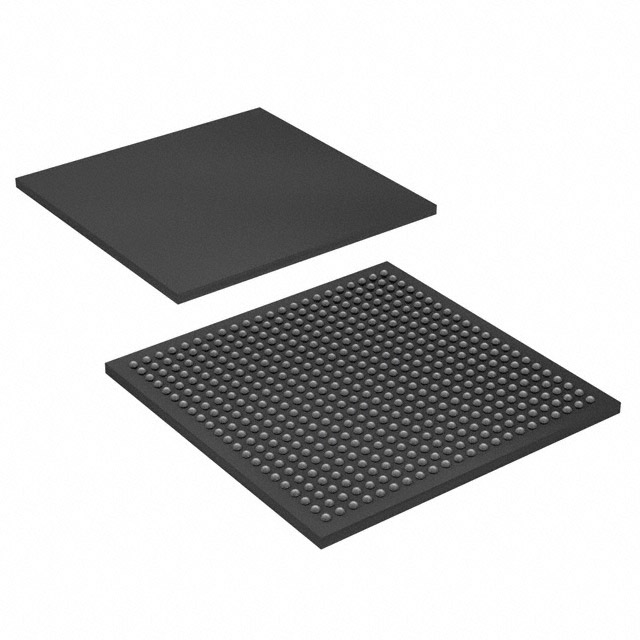
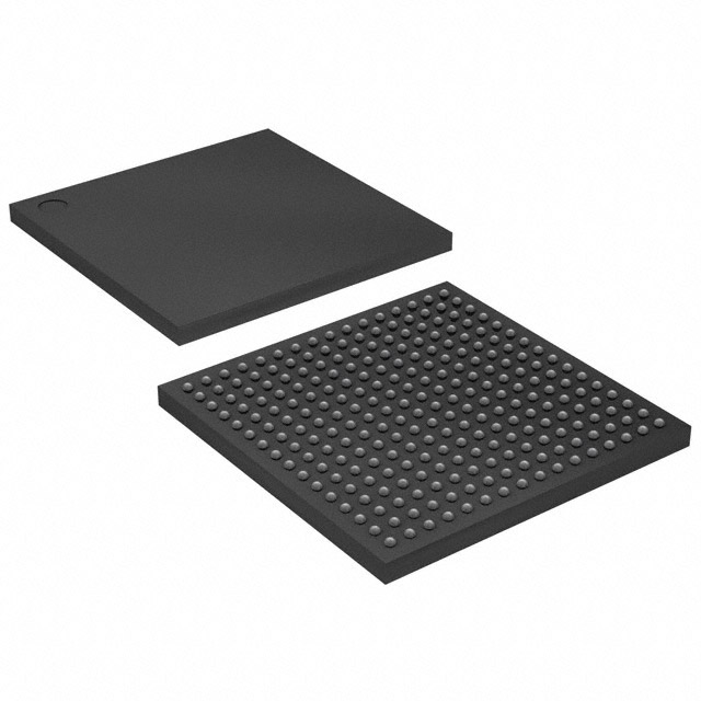
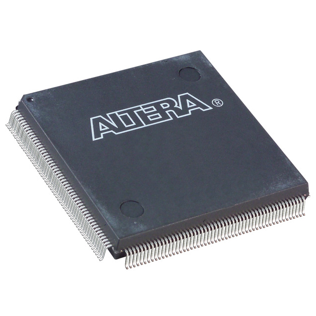
| Package / Case | 208-BFQFP | Number of I/O | 147 | Voltage | 2.375 V - 2.625 V | ||
| Mounting Method | Surface Mount | RoHS Compliance | RoHS non-compliant | REACH Compliance | REACH Unaffected | ||
| Moisture Sensitivity Level | 3 (168 Hours) | Number of LABs/CLBs | 624 | Number of Logic Elements/Cells | 4992 | ||
| Number of Gates | 257000 | ECCN | 3A991D | HTS Code | 8542.39.0001 | ||
| Qualification | N/A | Total RAM Bits | 49152 |
Overview of EP1K100QC208-1 – ACEX-1K® Field Programmable Gate Array (FPGA) IC 147 49152 4992 208-BFQFP
The EP1K100QC208-1 is an ACEX‑1K family FPGA offering programmable logic and embedded memory for system-level integration. It combines approximately 4,992 logic elements and about 49,152 bits of on-chip RAM with dedicated architectural features suited for SOPC-style integration and communications-focused designs.
This device is a commercial‑grade, surface‑mount FPGA in a 208‑BFQFP package that supports a 2.375–2.625 V supply and operates across a 0 °C to 70 °C temperature range, providing a compact, reconfigurable building block for mid-density digital designs.
Key Features
- Core Capacity Approximately 4,992 logic elements (LEs) and a maximum system gate equivalence of 257,000 for implementing moderate-complexity logic and control functions.
- Embedded Memory Approximately 49,152 bits of on-chip RAM with multiple embedded array blocks (EABs) that support efficient dual-port memory configurations.
- I/O and Voltage 147 user I/O pins with MultiVolt I/O capability described in the family datasheet; the device operates with an internal 2.5 V supply and requires an external supply in the 2.375 V to 2.625 V range.
- Package & Mounting 208‑BFQFP (supplier package: 208‑PQFP 28×28), surface‑mount mounting type for compact board layouts.
- System and Configuration Supports in-circuit reconfigurability (ICR) and includes JTAG boundary-scan test (IEEE 1149.1) circuitry available without consuming device logic.
- Clocking & Performance Features Built-in low-skew clock distribution trees, dedicated carry and cascade chains for arithmetic and high‑fan‑in logic, and options for ClockLock and ClockBoost to manage clock delay and skew (as described in the ACEX‑1K family documentation).
- Grade & Temperature Commercial grade, specified for operation from 0 °C to 70 °C.
- Standards & Interoperability Family-level documentation notes PCI Local Bus Specification compliance options for certain speed grades and MultiVolt I/O compatibility with 2.5 V, 3.3 V, and 5.0 V devices (refer to family datasheet for details).
Typical Applications
- Communications Interfaces Use for protocol bridging, packet buffering, and mid‑density datapath logic where embedded dual‑port RAM and deterministic interconnect are required.
- SOPC/System Integration Implement custom system‑on‑chip functions and glue logic to consolidate multiple discrete components into a single programmable device.
- Control and Timing Realize timing-critical control logic and arithmetic functions using dedicated carry/cascade chains and low‑skew clocking resources.
- Prototyping and Reconfigurable Logic Ideal for iterative development where in‑circuit reconfigurability and JTAG boundary-scan support streamline testing and updates.
Unique Advantages
- Balanced Logic and Memory Combines nearly 5,000 logic elements with about 49,152 bits of embedded RAM to support mixed logic and buffering needs without external memory in many designs.
- Flexible I/O and Voltage Support MultiVolt I/O options (family-level) and a defined external supply range (2.375–2.625 V) enable interfacing with a variety of system voltages.
- Reconfigurability and Testability In-circuit reconfigurability and integrated JTAG boundary-scan provide proven methods for updates and board-level test without consuming user logic.
- Compact Packaging 208‑pin BFQFP surface-mount package provides a space-efficient solution for board designs requiring moderate I/O count and logic density.
- Architectural Support for Arithmetic and High-Fan-In Logic Dedicated carry and cascade chains simplify implementation of fast adders, counters, and high fan-in functions, improving performance for common digital building blocks.
Why Choose EP1K100QC208-1?
The EP1K100QC208-1 delivers a practical balance of logic density, embedded memory, and system-level features in a commercial-grade FPGA package. Its combination of approximately 4,992 logic elements, embedded RAM, MultiVolt I/O capabilities, and reconfigurability makes it well suited for communications, SOPC integration, and control applications where compact form factor and flexible interfacing matter.
Designed for engineers who need a reprogrammable, testable, and compact FPGA option, this ACEX‑1K device provides a well-documented feature set and architectural building blocks that accelerate design implementation and simplify board-level integration.
Request a quote or submit a product inquiry today to get pricing, availability, and lead-time details for EP1K100QC208-1.


Date Founded: 1968
Headquarters: Santa Clara, California, USA
Employees: 130,000+
Revenue: $54.23 Billion
Certifications and Memberships: ISO9001:2015, ISO14001:2015, ISO17025:2017, ISO27001:2022, ISO45001:2018, ISO50001:2018


