
EP1K100QC208-3
| Part Description |
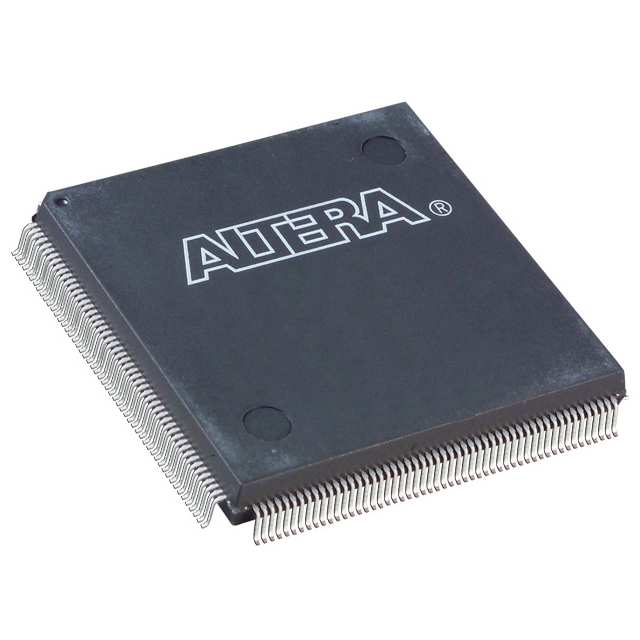
ACEX-1K® Field Programmable Gate Array (FPGA) IC 147 49152 4992 208-BFQFP |
|---|---|
| Quantity | 1,814 Available (as of June 10, 2026) |
| Product Category | Field Programmable Gate Array (FPGA) |
|---|---|
| Manufacturer | Intel |
| Manufacturing Status | Obsolete |
| Manufacturer Standard Lead Time | Contact Us |
| Datasheet |
Specifications & Environmental
| Device Package | 208-PQFP (28x28) | Grade | Commercial | Operating Temperature | 0°C – 70°C | ||
|---|---|---|---|---|---|---|---|
| Package / Case | 208-BFQFP | Number of I/O | 147 | Voltage | 2.375 V - 2.625 V | ||
| Mounting Method | Surface Mount | RoHS Compliance | RoHS non-compliant | REACH Compliance | REACH Unaffected | ||
| Moisture Sensitivity Level | 3 (168 Hours) | Number of LABs/CLBs | 624 | Number of Logic Elements/Cells | 4992 | ||
| Number of Gates | 257000 | ECCN | 3A991D | HTS Code | 8542.39.0001 | ||
| Qualification | N/A | Total RAM Bits | 49152 |
Overview of EP1K100QC208-3 – ACEX-1K® Field Programmable Gate Array (FPGA) IC, 208-BFQFP
The EP1K100QC208-3 is an ACEX-1K series field programmable gate array (FPGA) designed for commercial applications that require programmable logic and embedded memory in a single device. This device integrates approximately 4,992 logic elements, about 49,152 bits of embedded RAM, and up to 147 user I/O pins in a 208-BFQFP surface-mount package.
Targeted use cases include system-on-a-programmable-chip (SOPC) integration and communications or control applications that benefit from dense logic, dual-port embedded arrays, and flexible I/O voltage support. The part combines medium-high logic density and on-chip memory with features that simplify board-level integration and configuration.
Key Features
- Core Logic Approximately 4,992 logic elements and a typical device gate count of 100,000 (maximum system gates up to 257,000), enabling implementation of medium-density logic designs.
- Embedded Memory Approximately 49,152 total RAM bits delivered through embedded array blocks (EABs) that support dual-port operation and up to 16-bit widths per block for efficient on-chip data storage and megafunctions.
- I/O and Interface Flexibility Up to 147 user I/O pins with MultiVolt I/O capability noted in the ACEX-1K family; I/O features include programmable output slew-rate control, open-drain option, and pin-by-pin clamp to VCCIO options.
- Power and Supply Device designed to operate with an internal 2.5 V supply; specified supply range for this part is 2.375 V to 2.625 V.
- Package & Mounting 208-BFQFP (supplier device package: 208-PQFP, 28 × 28) in a surface-mount format for straightforward PCB assembly.
- Thermal and Grade Commercial-grade device with an operating temperature range of 0 °C to 70 °C.
- System & Configuration ACEX-1K family features include in-circuit reconfigurability (ICR), built-in JTAG boundary-scan, and dedicated carry and cascade chains to support arithmetic and high-fan-in logic functions (family-level capability).
- Design Support Family-level datasheet documents software design flows, megafunction support, and place-and-route tool compatibility (refer to the ACEX-1K documentation for details).
- Regulatory RoHS compliant.
Typical Applications
- Communications Systems Implements protocol glue logic, packet buffering and custom interfaces using embedded RAM and dedicated carry/cascade chains for high-speed logic functions.
- SOPC and Embedded Control Consolidates processor peripherals, custom state machines, and bus interfaces into a single programmable device to reduce BOM and board area.
- Memory-intensive Logic Uses the 49,152 bits of embedded RAM and dual-port EAB capability for FIFOs, lookup tables, and other on-chip data structures.
Unique Advantages
- Highly integrated logic and memory: Combines ~4,992 logic elements with ~49Kbits of embedded RAM to implement complex logic and data storage on-chip, reducing external component count.
- Flexible I/O signaling: MultiVolt family I/O capabilities and per-pin options allow easier interfacing with 2.5 V, 3.3 V, or 5.0 V systems at the board level.
- Board-friendly packaging: 208-BFQFP surface-mount package simplifies PCB layout and assembly for commercial products.
- Configurability and testability: In-circuit reconfigurability and built-in JTAG boundary-scan support streamline programming and board-level testing.
- Commercial temperature and supply suitability: Specified for 0 °C to 70 °C operation and a supply range of 2.375–2.625 V, matching typical commercial embedded designs.
Why Choose EP1K100QC208-3?
The EP1K100QC208-3 offers a balanced mix of logic density, embedded memory, and flexible I/O in a compact 208-BFQFP package, making it well suited for commercial SOPC, communications, and control designs that require on-chip RAM and moderate-to-high logic capacity. Its family-level features—such as dual-port EABs, dedicated arithmetic/cascade chains, JTAG boundary-scan, and in-circuit reconfigurability—help accelerate development and simplify system integration.
This device is targeted at designers seeking a commercial-grade FPGA solution with verified family support and documentation, enabling scalable designs that can leverage the ACEX-1K tool and megafunction ecosystem for implementation and testing.
Request a quote or submit an inquiry to get pricing and availability for EP1K100QC208-3 and to discuss how this FPGA can fit into your next design.


Date Founded: 1968
Headquarters: Santa Clara, California, USA
Employees: 130,000+
Revenue: $54.23 Billion
Certifications and Memberships: ISO9001:2015, ISO14001:2015, ISO17025:2017, ISO27001:2022, ISO45001:2018, ISO50001:2018


