
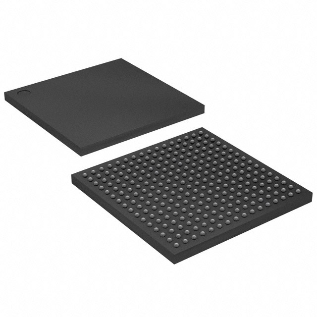
EP1K10FC256-1
| Part Description |
ACEX-1K® Field Programmable Gate Array (FPGA) IC 136 12288 576 256-BGA |
|---|---|
| Quantity | 1,291 Available (as of June 15, 2026) |

| Product Category | Field Programmable Gate Array (FPGA) |
|---|---|
| Manufacturer | Intel |
| Manufacturing Status | Obsolete |
| Manufacturer Standard Lead Time | Contact Us |
| Datasheet |
Specifications & Environmental
| Device Package | 256-FBGA (17x17) | Grade | Commercial | Operating Temperature | 0°C – 70°C | ||
|---|---|---|---|---|---|---|---|
| Package / Case | 256-BGA | Number of I/O | 136 | Voltage | 2.375 V - 2.625 V | ||
| Mounting Method | Surface Mount | RoHS Compliance | RoHS non-compliant | REACH Compliance | REACH Unaffected | ||
| Moisture Sensitivity Level | 3 (168 Hours) | Number of LABs/CLBs | 72 | Number of Logic Elements/Cells | 576 | ||
| Number of Gates | 56000 | ECCN | 3A991D | HTS Code | 8542.39.0001 | ||
| Qualification | N/A | Total RAM Bits | 12288 |
Overview of EP1K10FC256-1 – ACEX-1K FPGA, 256-BGA, 576 logic elements
The EP1K10FC256-1 is an ACEX-1K® field programmable gate array (FPGA) in a 256-ball fine-pitch BGA package designed for commercial-temperature applications. It combines a logic array with embedded array blocks (EABs) to deliver programmable logic and on-chip memory for system-on-a-programmable-chip (SOPC) integration, making it suitable for cost-sensitive, high-volume designs.
This device supports multi-voltage I/O and an internal 2.5 V core supply, offering flexible interfacing and integration options for communications, protocol bridging, buffering, and other embedded digital functions.
Key Features
- Logic Resources — 576 logic elements (LEs) providing the programmable fabric for custom logic and glue-logic implementations.
- Embedded Memory — 12,288 total RAM bits implemented across EABs to support efficient on-chip buffering and megafunctions; EABs include dual-port capability.
- System Gates — Up to 56,000 maximum system gates for mapping moderate-density designs.
- I/O Flexibility — 136 user I/O pins with MultiVolt capability to interface with 2.5 V, 3.3 V, or 5.0 V devices and per-pin options such as open-drain and programmable output slew-rate control.
- Configuration & Test — JTAG boundary-scan (IEEE 1149.1) and in-circuit reconfigurability (ICR) support via external configuration devices or JTAG port for field updates and testability.
- Clocking & Interconnect — Built-in low-skew clock distribution, dedicated carry and cascade chains for arithmetic and high-fan-in logic, and FastTrack® continuous routing for predictable interconnect delays.
- Package & Supply — 256-ball fine-pitch BGA (256-FBGA, 17×17) surface-mount package; device operates with a core supply around 2.5 V (specified supply range 2.375 V to 2.625 V).
- Commercial Temperature & Compliance — Commercial grade operation from 0 °C to 70 °C and RoHS compliant.
Typical Applications
- Communications Interfaces — Implement protocol bridging, data path logic, and buffering using the device’s EABs and dedicated carry/cascade chains for deterministic performance.
- System-on-a-Programmable-Chip (SOPC) — Integrate custom logic, memory functions, and peripheral glue logic in a single FPGA to reduce board-level component count.
- PCI and Bus Interface Logic — Support for PCI Local Bus operation at 3.3 V (33 MHz or 66 MHz) for compliant bus-interface implementations on -1 speed grade devices.
- On-chip Dual-Port Memory — Use embedded array blocks for efficient dual-port memory and megafunction implementations such as FIFOs and small buffers.
Unique Advantages
- Balanced Integration: Combines 576 logic elements with 12,288 bits of embedded memory to implement control, datapath, and storage functions on a single device.
- Flexible I/O Standards: MultiVolt I/O enables direct interfacing with 2.5 V, 3.3 V, or 5.0 V systems, reducing the need for external level translators.
- Field Reconfigurability and Test: JTAG boundary-scan and in-circuit reconfigurability simplify board-level testing and firmware updates in the field.
- Deterministic Arithmetic & Routing: Dedicated carry and cascade chains plus FastTrack® interconnect provide predictable timing for arithmetic and high-fan-in functions.
- Compact, Surface-Mount Package: 256-FBGA (17×17) package offers high pin density in a compact footprint for space-constrained PCBs.
- Regulatory & Environmental Readiness: RoHS compliance supports environmentally conscious designs and supply-chain requirements.
Why Choose EP1K10FC256-1?
The EP1K10FC256-1 positions itself as a compact, commercially graded FPGA option for designers needing moderate logic capacity with on-chip memory and flexible I/O. Its combination of 576 logic elements, 12,288 bits of embedded RAM, and up to 136 I/O pins makes it well suited for SOPC integration, interface logic, and communications-related functions in cost-sensitive designs.
Backing these capabilities is a family-level architecture that includes features such as low-skew clocking, dedicated arithmetic chains, and standard test/configuration interfaces, enabling scalable migration within the ACEX-1K family while maintaining pin compatibility across FineLine BGA options.
Request a quote or submit a pricing inquiry to receive availability and lead-time information for the EP1K10FC256-1.


Date Founded: 1968
Headquarters: Santa Clara, California, USA
Employees: 130,000+
Revenue: $54.23 Billion
Certifications and Memberships: ISO9001:2015, ISO14001:2015, ISO17025:2017, ISO27001:2022, ISO45001:2018, ISO50001:2018


