
EP1K10FC256-2
| Part Description |
ACEX-1K® Field Programmable Gate Array (FPGA) IC 136 12288 576 256-BGA |
|---|---|
| Quantity | 1,254 Available (as of June 9, 2026) |

| Product Category | Field Programmable Gate Array (FPGA) |
|---|---|
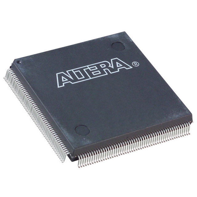
| Manufacturer | Intel |
| Manufacturing Status | Obsolete |
| Manufacturer Standard Lead Time | Contact Us |
| Datasheet |
Specifications & Environmental
| Device Package | 256-FBGA (17x17) | Grade | Commercial | Operating Temperature | 0°C – 70°C | ||
|---|---|---|---|---|---|---|---|
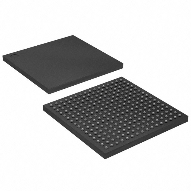
| Package / Case | 256-BGA | Number of I/O | 136 | Voltage | 2.375 V - 2.625 V | ||
| Mounting Method | Surface Mount | RoHS Compliance | RoHS non-compliant | REACH Compliance | REACH Unaffected | ||
| Moisture Sensitivity Level | 3 (168 Hours) | Number of LABs/CLBs | 72 | Number of Logic Elements/Cells | 576 | ||
| Number of Gates | 56000 | ECCN | 3A991D | HTS Code | 8542.39.0001 | ||
| Qualification | N/A | Total RAM Bits | 12288 |
Overview of EP1K10FC256-2 – ACEX-1K Field Programmable Gate Array, 256‑BGA
The EP1K10FC256-2 is a commercial-grade ACEX-1K family FPGA providing a compact, programmable logic solution for system integration and high-volume applications. Built around the ACEX 1K architecture, the device combines dedicated embedded memory, a logic array, and flexible I/O to support communications, SOPC-style integration, and general-purpose logic functions.
With 576 logic elements, 12,288 bits of embedded RAM and up to 136 user I/Os in a 256‑BGA package, this device targets designs that require moderate logic density, on-chip memory and multi‑voltage I/O capability in a surface-mount form factor.
Key Features
- Core Logic — 576 logic elements (LEs) delivering programmable logic capacity suitable for control, glue-logic, and medium-density FPGA functions.
- Embedded Memory — Approximately 12,288 bits of on-chip RAM implemented via Embedded Array Blocks (EABs) with dual-port capability and support for up to 16-bit width per EAB.
- Logic Density & Gates — Device supports up to 56,000 system gates, aligning with ACEX-1K family characteristics for medium-density integration.
- I/O and MultiVolt Support — Up to 136 user I/O pins with MultiVolt I/O capability (family-level feature) to interface with 2.5‑V, 3.3‑V, or 5.0‑V devices; programmable slew-rate and per-pin output options are supported by the family architecture.
- Power and Supply — Operates with an internal 2.5‑V supply; specified external supply range 2.375 V to 2.625 V for core operation.
- Packaging & Mounting — Available in a 256‑BGA surface-mount package (supplier device package: 256‑FBGA 17×17) for compact board-level integration.
- Configuration & Test — In-circuit reconfigurability and built-in JTAG boundary-scan test (IEEE 1149.1) as part of the ACEX‑1K family feature set, enabling field updates and board-level testability without consuming user logic.
- Clock & Interconnect — Family-level features include low-skew clock distribution, dedicated carry and cascade chains for arithmetic and high‑fan-in functions, and a continuous routing structure for predictable interconnect delays.
- Compliance & Environmental — RoHS compliant; commercial-grade device with an operating temperature range of 0 °C to 70 °C.
Typical Applications
- Communications Equipment — Implement protocol logic, data routing and interface bridging where moderate gate counts and embedded memory are needed.
- System-on-a-Programmable-Chip (SOPC) — Integrate specialized logic functions and on-chip memory to consolidate multiple functions into a single programmable device.
- Peripheral and Interface Control — Use for bus interfacing, glue logic, and peripheral controllers taking advantage of the device’s flexible I/O and in-circuit reconfigurability.
- Embedded Memory Functions — Implement small dual-port RAM blocks, lookup tables, and FIFO buffers using the EAB resources for compact on-chip storage.
Unique Advantages
- Balanced Logic and Memory: 576 logic elements combined with 12,288 bits of embedded RAM provide a well-balanced resource mix for control-oriented and memory-assisted functions.
- Flexible I/O Integration: Up to 136 user I/Os with MultiVolt family support enable direct interfacing to a wide range of peripherals and legacy devices.
- Compact, Surface‑Mount Package: The 256‑BGA (256‑FBGA 17×17) package delivers a small board footprint for space-constrained applications.
- Field Reconfigurability and Testability: Built-in JTAG and in‑circuit reconfiguration support facilitate field updates and reduce development and maintenance complexity.
- Commercial Temperature and RoHS Compliance: Rated for 0 °C to 70 °C operation and RoHS compliant for environmental and supply-chain alignment.
Why Choose EP1K10FC256-2?
The EP1K10FC256-2 positions itself as a compact, commercially graded FPGA that combines moderate logic capacity, embedded memory and flexible I/O in a 256‑BGA surface-mount package. It is well suited to engineers designing communications interfaces, SOPC integration points, or peripheral controllers where on-chip RAM and reconfigurability simplify board-level design.
Leveraging ACEX-1K family features—such as dual-port EABs, dedicated carry/cascade chains, and JTAG-based configuration—the EP1K10FC256-2 delivers predictable integration and testability, making it a practical choice for volume designs that require a programmable, mid-density logic device.
Request a quote or submit a purchase inquiry to receive pricing, availability, and additional ordering information for the EP1K10FC256-2.


Date Founded: 1968
Headquarters: Santa Clara, California, USA
Employees: 130,000+
Revenue: $54.23 Billion
Certifications and Memberships: ISO9001:2015, ISO14001:2015, ISO17025:2017, ISO27001:2022, ISO45001:2018, ISO50001:2018


