
EP1K100QI208-2N
| Part Description |
ACEX-1K® Field Programmable Gate Array (FPGA) IC 147 49152 4992 208-BFQFP |
|---|---|
| Quantity | 178 Available (as of June 10, 2026) |

| Product Category | Field Programmable Gate Array (FPGA) |
|---|---|
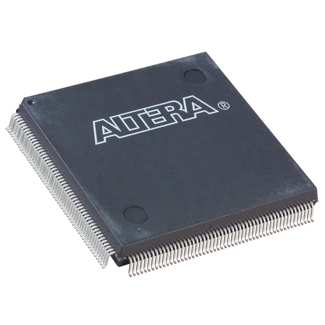
| Manufacturer | Intel |
| Manufacturing Status | Obsolete |
| Manufacturer Standard Lead Time | Contact Us |
| Datasheet |
Specifications & Environmental
| Device Package | 208-PQFP (28x28) | Grade | Industrial | Operating Temperature | -40°C – 85°C | ||
|---|---|---|---|---|---|---|---|
| Package / Case | 208-BFQFP | Number of I/O | 147 | Voltage | 2.375 V - 2.625 V | ||
| Mounting Method | Surface Mount | RoHS Compliance | Unknown | REACH Compliance | REACH Unaffected | ||
| Moisture Sensitivity Level | 3 (168 Hours) | Number of LABs/CLBs | 624 | Number of Logic Elements/Cells | 4992 | ||
| Number of Gates | 257000 | ECCN | 3A991D | HTS Code | 8542.39.0001 | ||
| Qualification | N/A | Total RAM Bits | 49152 |
Overview of EP1K100QI208-2N – ACEX-1K® Field Programmable Gate Array (FPGA) IC 147 49152 4992 208-BFQFP
The EP1K100QI208-2N is an ACEX-1K family field programmable gate array (FPGA) in a 208-pin BFQFP package, designed for mid-density programmable logic integration. It combines a logic array with embedded array blocks (EABs) to implement memory-intensive megafunctions and general-purpose logic on a single surface-mount device.
Typical use cases include system-on-a-programmable-chip (SOPC) integration, communications and industrial systems that require reconfigurable logic, embedded RAM, and flexible I/O. The device provides a balance of logic density, on-chip memory, and industrial temperature operation for reliable deployment.
Key Features
- Logic Capacity — 4,992 logic elements (LEs) and approximately 257,000 maximum system gates provide mid-range programmable logic resources for glue logic, control, and custom datapaths.
- Embedded Memory (EABs) — Up to 12 embedded array blocks (EABs) with a total of 49,152 RAM bits (4,096 bits per EAB) and dual-port capability for implementing efficient on-chip buffers, FIFOs, and memory-based megafunctions.
- I/O Flexibility — 147 user I/O pins in the 208-BFQFP package support mixed-signal interfacing and external device connections in compact board designs.
- Dedicated Arithmetic and Logic Chains — Built-in carry and cascade chains accelerate adders, counters, comparators, and high-fan-in logic without consuming excess general routing resources.
- Configuration and Test — JTAG boundary-scan (IEEE 1149.1) and in-circuit reconfigurability support device programming, debug, and manufacturing test workflows.
- Package & Mounting — 208-BFQFP (supplier device package 208-PQFP, 28×28) surface-mount package suitable for compact PCB layouts.
- Power and Supply — Device internal supply range specified at 2.375 V to 2.625 V; designed to operate with a 2.5 V internal supply architecture.
- Industrial Temperature Range — Rated for operation from −40 °C to 85 °C for deployment in industrial environments.
- Compliance & Environmental — RoHS-compliant design for regulatory and manufacturing requirements.
Typical Applications
- System-on-a-Programmable-Chip (SOPC) — Integrate memory blocks and custom logic into a single FPGA to reduce board-level component count and simplify system architecture.
- Communications Equipment — Implement protocol handling, buffering, and specialized logic using the device's embedded RAM and dedicated arithmetic chains.
- PCI and Bus Interface Prototyping — Use the device for prototyping and interfacing bus logic and peripheral controllers where reconfigurable logic and embedded memory are needed.
- Industrial Control — Deploy in control and automation systems that require industrial temperature operation and a reconfigurable logic platform.
Unique Advantages
- Highly integrated mid-density FPGA: 4,992 logic elements with 49,152 bits of embedded RAM deliver a compact combination of logic and memory for space-constrained designs.
- Memory-efficient EAB architecture: Twelve EABs with dual-port capability enable efficient implementation of FIFOs, lookup tables, and memory-backed megafunctions without sacrificing logic capacity.
- Flexible I/O in a compact package: 147 user I/O pins in a 208-BFQFP surface-mount package make it suitable for dense board layouts while maintaining connectivity options.
- Design-for-test and reconfiguration: JTAG boundary-scan and in-circuit reconfigurability simplify manufacturing test, in-field updates, and iterative development.
- Industrial readiness: Rated for −40 °C to 85 °C and RoHS-compliant, supporting deployment in industrial environments with regulatory compliance.
- Deterministic arithmetic support: Dedicated carry and cascade chains reduce resource usage and improve performance for arithmetic and high-fan-in functions.
Why Choose EP1K100QI208-2N?
The EP1K100QI208-2N provides a balanced FPGA solution for engineers who need mid-range logic density, substantial on-chip memory, and industrial temperature operation in a compact surface-mount package. Its combination of 4,992 logic elements, 49,152 RAM bits across embedded array blocks, and 147 user I/Os makes it well suited to SOPC integration, communications logic, and industrial control applications.
Backed by ACEX-1K family features such as dedicated arithmetic chains, JTAG testability, and in-circuit reconfigurability, this Intel-manufactured device supports iterative development and field updates while helping reduce board-level component count and complexity.
Request a quote or submit an inquiry to receive pricing, availability, and technical support information for EP1K100QI208-2N.


Date Founded: 1968
Headquarters: Santa Clara, California, USA
Employees: 130,000+
Revenue: $54.23 Billion
Certifications and Memberships: ISO9001:2015, ISO14001:2015, ISO17025:2017, ISO27001:2022, ISO45001:2018, ISO50001:2018


