
EP1K100QC208-3N
| Part Description |
ACEX-1K® Field Programmable Gate Array (FPGA) IC 147 49152 4992 208-BFQFP |
|---|---|
| Quantity | 905 Available (as of June 15, 2026) |

| Product Category | Field Programmable Gate Array (FPGA) |
|---|---|
| Manufacturer | Intel |
| Manufacturing Status | Obsolete |
| Manufacturer Standard Lead Time | Contact Us |
| Datasheet |
Specifications & Environmental
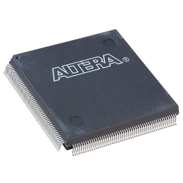
| Device Package | 208-PQFP (28x28) | Grade | Commercial | Operating Temperature | 0°C – 70°C | ||
|---|---|---|---|---|---|---|---|
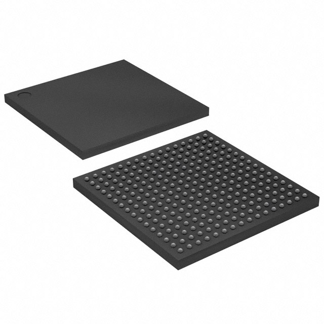
| Package / Case | 208-BFQFP | Number of I/O | 147 | Voltage | 2.375 V - 2.625 V | ||
| Mounting Method | Surface Mount | RoHS Compliance | Unknown | REACH Compliance | REACH Unaffected | ||
| Moisture Sensitivity Level | 3 (168 Hours) | Number of LABs/CLBs | 624 | Number of Logic Elements/Cells | 4992 | ||
| Number of Gates | 257000 | ECCN | 3A991D | HTS Code | 8542.39.0001 | ||
| Qualification | N/A | Total RAM Bits | 49152 |
Overview of EP1K100QC208-3N – ACEX-1K® Field Programmable Gate Array (FPGA) IC 147 49152 4992 208-BFQFP
The EP1K100QC208-3N is an ACEX-1K family field programmable gate array (FPGA) optimized for commercial, cost-sensitive system-on-a-programmable-chip (SOPC) designs. It combines a mid-density logic array with embedded memory and flexible I/O to implement control, glue-logic, and memory-centric megafunctions in a single surface-mount device.
This device is targeted at commercial applications that require approximately 4,992 logic elements, on-chip embedded memory, and a substantial I/O count, while operating from a 2.375 V to 2.625 V supply across a 0 °C to 70 °C range.
Key Features
- Core logic — 4,992 logic elements providing a typical density equivalent to approximately 257,000 gates for mid-range logic integration.
- Embedded memory (EABs) — Up to 49,152 total RAM bits with dual-port capability and support for megafunctions; EAB architecture enables efficient on-chip storage and specialized logic functions.
- I/O and interfacing — 147 user I/O pins with MultiVolt-compatible family I/O options; individual tri-state control, open-drain option, and programmable slew-rate control are supported by the ACEX-1K family.
- Clocking and timing — Built-in low-skew clock distribution with options such as ClockLock and ClockBoost, and support for multiple global clocks and global clear signals for synchronized designs.
- Configuration and test — In-circuit reconfigurability via external configuration devices or JTAG; JTAG boundary-scan (IEEE Std. 1149.1) is available without consuming device logic.
- Power and supply — Operates from a specified supply range of 2.375 V to 2.625 V; device family emphasizes low power consumption and cost-optimized process technology.
- Package and mounting — 208-BFQFP package case, surface-mount mounting; supplier device package listed as 208-PQFP (28×28).
- Commercial grade and compliance — Commercial temperature rating (0 °C to 70 °C) and RoHS-compliant for regulatory cleanliness.
Typical Applications
- Communications equipment — Implement protocol glue logic, packet buffering, and control functions using on-chip memory and flexible logic resources.
- Embedded controllers and SOPC — Integrate peripheral control, state machines, and small processors with embedded dual-port memory for compact system designs.
- Consumer and commercial electronics — Use the FPGA for custom logic, interface adaptation, and feature-rich control in cost-sensitive product lines.
- Prototyping and product migration — Mid-density logic and a comprehensive feature set make this device suitable for validating designs that later scale within the ACEX-1K family.
Unique Advantages
- Balanced integration: Combines nearly 5,000 logic elements with 49,152 RAM bits to consolidate functions that would otherwise require multiple components, reducing system BOM and board area.
- Flexible memory architecture: Embedded array blocks with dual-port support enable efficient implementation of FIFOs, buffers, and small memories without sacrificing logic capacity.
- Robust I/O capabilities: Family-level MultiVolt I/O features and per-pin options (tri-state, open-drain, slew control) simplify interfacing to a variety of external devices.
- Design and test support: JTAG boundary-scan and in-circuit reconfigurability streamline manufacturing test and field updates while preserving usable logic resources.
- Commercial readiness: Surface-mount 208-pin package, commercial temperature rating, and RoHS compliance align with mainstream electronics production and regulatory requirements.
- Vendor tool ecosystem: ACEX-1K family supports standard design flows and automated place-and-route tools to accelerate development and reduce time to market.
Why Choose EP1K100QC208-3N?
The EP1K100QC208-3N offers a practical mid-density FPGA option for commercial designs that need a balance of logic capacity, on-chip memory, and flexible I/O in a 208-pin surface-mount package. Its combination of approximately 4,992 logic elements, 49,152 RAM bits, and 147 I/O pins supports consolidated system integration while maintaining a commercial-grade operating range and RoHS compliance.
Designers and product teams targeting communications, embedded controllers, and compact SOPC implementations will find the device's reconfigurability, memory architecture, and clocking options valuable for reducing component count and accelerating development with supported design tools.
Request a quote or submit an inquiry to obtain pricing and availability for the EP1K100QC208-3N.


Date Founded: 1968
Headquarters: Santa Clara, California, USA
Employees: 130,000+
Revenue: $54.23 Billion
Certifications and Memberships: ISO9001:2015, ISO14001:2015, ISO17025:2017, ISO27001:2022, ISO45001:2018, ISO50001:2018


