
EP1K10FC256-3
| Part Description |
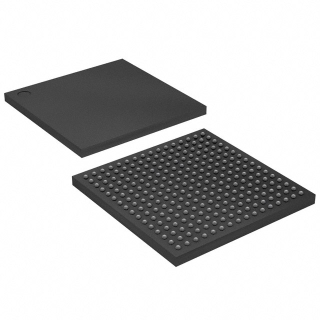
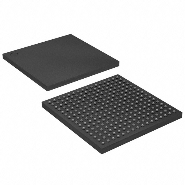
ACEX-1K® Field Programmable Gate Array (FPGA) IC 136 12288 576 256-BGA |
|---|---|
| Quantity | 244 Available (as of October 8, 2026) |

| Product Category | Field Programmable Gate Array (FPGA) |
|---|---|
| Manufacturer | Intel |
| Manufacturing Status | Obsolete |
| Manufacturer Standard Lead Time | Contact Us |
| Datasheet |
Specifications & Environmental
| Device Package | 256-FBGA (17x17) | Grade | Commercial | Operating Temperature | 0°C – 70°C | ||
|---|---|---|---|---|---|---|---|
| Package / Case | 256-BGA | Number of I/O | 136 | Voltage | 2.375 V - 2.625 V | ||
| Mounting Method | Surface Mount | RoHS Compliance | RoHS non-compliant | REACH Compliance | REACH Unaffected | ||
| Moisture Sensitivity Level | 3 (168 Hours) | Number of LABs/CLBs | 72 | Number of Logic Elements/Cells | 576 | ||
| Number of Gates | 56000 | ECCN | 3A991D | HTS Code | 8542.39.0001 | ||
| Qualification | N/A | Total RAM Bits | 12288 |
Overview of EP1K10FC256-3 – ACEX-1K® Field Programmable Gate Array (FPGA), 576 logic elements, 12,288-bit embedded RAM, 136 I/O, 256-BGA
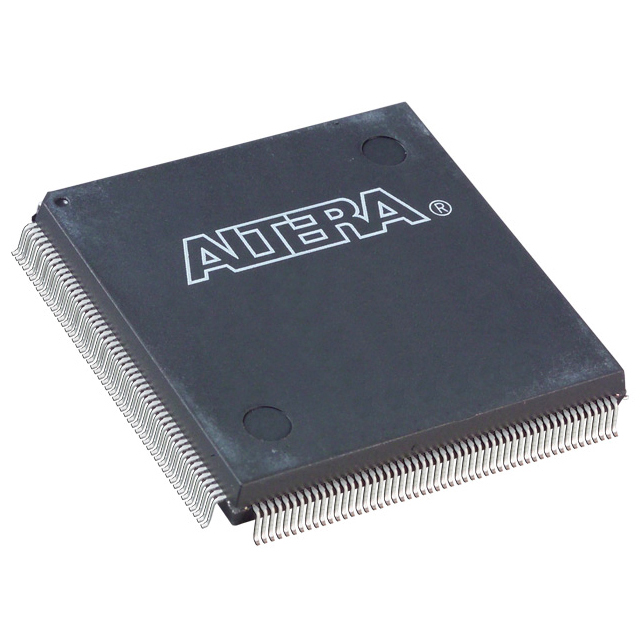
The EP1K10FC256-3 is an ACEX-1K® FPGA family device delivering reconfigurable logic and embedded memory in a compact 256-FBGA (17×17) package. Built for commercial applications, this device combines 576 logic elements with approximately 12,288 bits of on-chip RAM and 136 user I/Os to enable system-on-programmable-chip integration, memory-mapped functions, and general-purpose logic processing.
Designed for cost-efficient, low-power implementations, the device supports in-circuit reconfigurability and JTAG boundary-scan for board-level test and configuration. Its electrical and package specifications make it suitable for a range of commercial communications and embedded control applications.
Key Features
- Core Logic 576 logic elements (LEs) provide combinational and sequential resources for implementing custom logic, state machines, and peripheral glue logic.
- Embedded Memory Approximately 12,288 bits of on-chip RAM for data buffering, small FIFOs, and lookup tables.
- I/O Density 136 user I/O pins support interfacing to external devices and peripherals in a compact BGA footprint.
- Package & Mounting 256-FBGA (17×17) package in a surface-mount form factor for PCB designs with a small board area budget.
- Power Supply Specified supply range of 2.375 V to 2.625 V with an internal 2.5-V core supply as documented for the ACEX-1K family.
- Temperature & Grade Commercial grade operation from 0 °C to 70 °C.
- Configuration & Test In-circuit reconfigurability and JTAG boundary-scan (IEEE 1149.1) support for configuration, programming, and board-level test.
- Flexible I/O & System Features ACEX-1K family features cited in the datasheet include MultiVolt I/O options, individual tri-state control, open-drain options, and programmable slew-rate control to tailor I/O behavior.
- Interconnect & Arithmetic Support Series architecture includes dedicated carry and cascade chains and FastTrack interconnect to support arithmetic functions and predictable routing.
- RoHS Compliant Device is RoHS compliant for lead-free manufacturing workflows.
Typical Applications
- Communications Equipment Use the device for glue logic, protocol bridging, and small packet buffering where compact FPGA resources and reconfigurability are needed.
- Embedded Control Implement control state machines, peripheral interfaces, and timing-critical logic in consumer and commercial embedded systems.
- System Integration / SOPC Integrate memory-mapped functions and custom logic to reduce board-level component count in system-on-a-programmable-chip designs.
- Board-Level Test & In-System Updates Leverage JTAG boundary-scan and in-circuit reconfigurability for diagnostics, firmware updates, and manufacturing test flows.
Unique Advantages
- Compact, reconfigurable platform: 576 logic elements and embedded RAM allow implementation of moderate-complexity functions in a single 256-FBGA device, reducing BOM and PCB area.
- Flexible I/O options: 136 I/Os and MultiVolt I/O capabilities let you interface with a variety of peripheral voltage domains without adding level-shifting components.
- Board-level testability: IEEE 1149.1 JTAG boundary-scan support enables streamlined production testing and in-system programming.
- Predictable arithmetic and routing support: Dedicated carry and cascade chains with FastTrack interconnect simplify implementation of adders, counters, and other high-fan-in logic.
- Commercial-grade reliability: Specified operating range of 0 °C to 70 °C and RoHS compliance align with commercial production and regulatory expectations.
- Toolchain and ecosystem support: ACEX-1K family design support (as documented) enables integration with common FPGA development flows for synthesis, place-and-route, and simulation.
Why Choose EP1K10FC256-3?
The EP1K10FC256-3 delivers a balanced mix of reconfigurable logic, embedded RAM, and I/O density in a compact 256-FBGA package suited for commercial communications and embedded designs. Its on-chip resources and configuration features make it a practical choice when board space, flexibility, and in-system update capability are priorities.
For designers seeking a cost-efficient, RoHS-compliant FPGA with JTAG testability, MultiVolt I/O support, and predictable interconnect/arithmetical resources, the EP1K10FC256-3 provides a field-programmable building block that integrates with existing FPGA development toolchains and production test flows.
Request a quote or submit an inquiry to receive pricing, lead-time, and availability for the EP1K10FC256-3 and to discuss volume or technical requirements.

























Date Founded: 1968
Headquarters: Santa Clara, California, USA
Employees: 130,000+
Revenue: $54.23 Billion
Certifications and Memberships: ISO9001:2015, ISO14001:2015, ISO17025:2017, ISO27001:2022, ISO45001:2018, ISO50001:2018


