
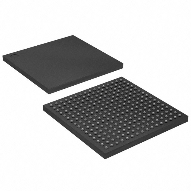
EP1K10FI256-2N
| Part Description |
ACEX-1K® Field Programmable Gate Array (FPGA) IC 136 12288 576 256-BGA |
|---|---|
| Quantity | 236 Available (as of June 14, 2026) |

| Product Category | Field Programmable Gate Array (FPGA) |
|---|---|
| Manufacturer | Intel |
| Manufacturing Status | Obsolete |
| Manufacturer Standard Lead Time | Contact Us |
| Datasheet |
Specifications & Environmental
| Device Package | 256-FBGA (17x17) | Grade | Industrial | Operating Temperature | -40°C – 85°C | ||
|---|---|---|---|---|---|---|---|
| Package / Case | 256-BGA | Number of I/O | 136 | Voltage | 2.375 V - 2.625 V | ||
| Mounting Method | Surface Mount | RoHS Compliance | Unknown | REACH Compliance | REACH Unaffected | ||
| Moisture Sensitivity Level | 3 (168 Hours) | Number of LABs/CLBs | 72 | Number of Logic Elements/Cells | 576 | ||
| Number of Gates | 56000 | ECCN | 3A991D | HTS Code | 8542.39.0001 | ||
| Qualification | N/A | Total RAM Bits | 12288 |
Overview of EP1K10FI256-2N – ACEX-1K Field Programmable Gate Array (FPGA), 256-BGA
The EP1K10FI256-2N is an Intel ACEX-1K family programmable logic device in a 256-ball FineLine BGA package. It combines a logic array with embedded memory and dedicated routing to support system-on-programmable-chip (SOPC) integration for communication and embedded applications.
Designed for industrial use, this device provides 576 logic elements, 12,288 bits of embedded RAM, up to 136 user I/O pins, and an operating range suited for robust board-level designs. Key system features include multi-voltage I/O support, in-circuit reconfigurability, and built-in boundary-scan for testability.
Key Features
- Core logic — 576 logic elements delivering general-purpose combinational and sequential logic for glue logic, state machines, and control functions.
- Embedded memory — 12,288 bits of on-chip RAM for buffers, small tables, and dual-port memory implementations.
- I/O capability — Up to 136 user I/O pins with MultiVolt I/O support (can drive or be driven by 2.5 V, 3.3 V, or 5.0 V devices) and per-pin programmable slew-rate and open-drain options.
- Performance and routing — Dedicated carry and cascade chains plus FastTrack interconnect for predictable, high-speed arithmetic and high-fan-in logic.
- Configuration and test — In-circuit reconfigurability (ICR) via external configuration devices or JTAG, and built-in IEEE 1149.1-compliant boundary-scan circuitry for board-level test without consuming device logic.
- Clocking and timing — Built-in low-skew clock distribution with ClockLock and ClockBoost options to reduce clock delay and skew where required.
- Package and thermal — Surface-mount 256-FBGA (17 × 17) package, industrial temperature grade with an operating range of −40 °C to 85 °C.
- Power — Operates with an internal 2.5 V supply; recommended external supply range 2.375 V to 2.625 V for core power.
Typical Applications
- Communications equipment — Implement protocol bridging, packet parsing, and interface glue logic where compact, reconfigurable logic and embedded RAM are required.
- Embedded control — Control logic, state machines, and I/O aggregation in industrial controllers and automation systems using the device’s logic elements and I/O flexibility.
- Peripheral interfacing — Level-shifting and buffering between mixed-voltage peripherals with MultiVolt I/O support and programmable pin options.
- Low-to-mid density SOPC integration — Integrate custom logic, small memory blocks, and interface functions into a single programmable device to reduce board-level component count.
Unique Advantages
- Compact, high-density integration: 576 logic elements and 12,288 bits of embedded RAM enable consolidation of discrete logic and small memory functions into a single IC.
- Flexible I/O for mixed-voltage systems: MultiVolt I/O support (2.5 V/3.3 V/5.0 V) simplifies interoperability with a wide range of legacy and modern peripherals.
- Board-level test and reconfiguration: Built-in JTAG boundary-scan and in-circuit reconfigurability streamline production test and field updates without consuming user logic.
- Predictable arithmetic and routing: Dedicated carry and cascade chains with FastTrack interconnect reduce critical-path delays for adders, counters, and high-fan-in functions.
- Industrial-grade operation: Surface-mount 256-FBGA package and −40 °C to 85 °C rating support deployment in industrial temperature environments.
Why Choose EP1K10FI256-2N?
The EP1K10FI256-2N delivers a balanced combination of logic capacity, embedded memory, and flexible I/O in a compact 256-BGA package tailored for industrial applications. Its mix of configurable logic, on-chip RAM, MultiVolt I/O, and built-in test and reconfiguration features makes it suitable for designers who need to consolidate discrete components and enable in-field updates.
This device is appropriate for development teams building communication interfaces, embedded controllers, and SOPC-based solutions that require reliable, reprogrammable logic with predictable routing and dedicated arithmetic resources. Its industrial temperature rating and surface-mount FBGA package support durable board-level deployment and production test flows.
Request a quote or submit an inquiry to receive pricing and availability details for EP1K10FI256-2N and to discuss how this ACEX-1K FPGA can fit into your next design.


Date Founded: 1968
Headquarters: Santa Clara, California, USA
Employees: 130,000+
Revenue: $54.23 Billion
Certifications and Memberships: ISO9001:2015, ISO14001:2015, ISO17025:2017, ISO27001:2022, ISO45001:2018, ISO50001:2018


