
EP1K30QC208-3
| Part Description |
ACEX-1K® Field Programmable Gate Array (FPGA) IC 147 24576 1728 208-BFQFP |
|---|---|
| Quantity | 214 Available (as of June 15, 2026) |

| Product Category | Field Programmable Gate Array (FPGA) |
|---|---|
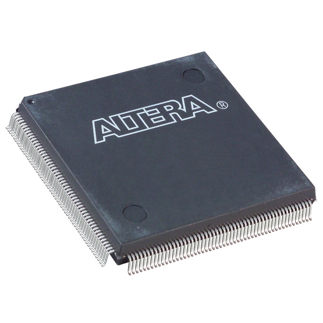
| Manufacturer | Intel |
| Manufacturing Status | Obsolete |
| Manufacturer Standard Lead Time | Contact Us |
| Datasheet |
Specifications & Environmental
| Device Package | 208-PQFP (28x28) | Grade | Commercial | Operating Temperature | 0°C – 70°C | ||
|---|---|---|---|---|---|---|---|
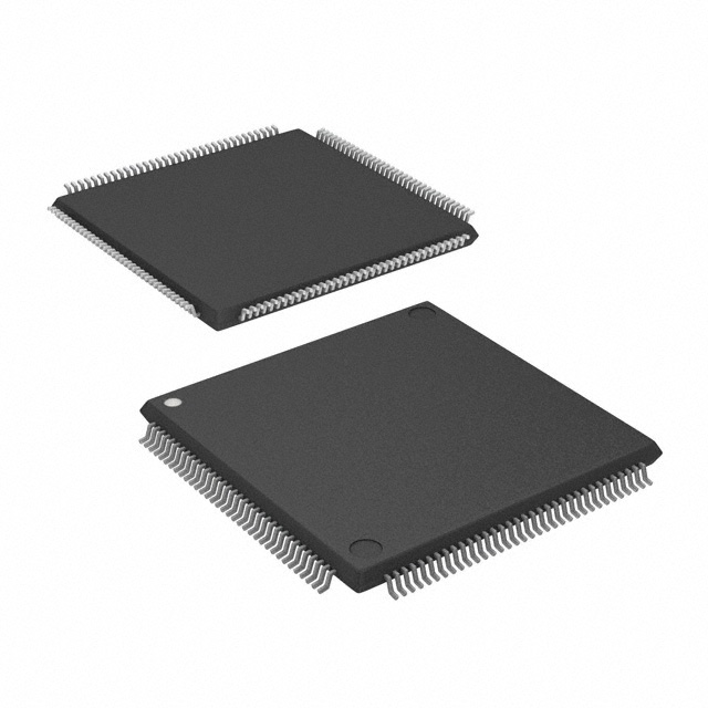
| Package / Case | 208-BFQFP | Number of I/O | 147 | Voltage | 2.375 V - 2.625 V | ||
| Mounting Method | Surface Mount | RoHS Compliance | RoHS non-compliant | REACH Compliance | REACH Unaffected | ||
| Moisture Sensitivity Level | 3 (168 Hours) | Number of LABs/CLBs | 216 | Number of Logic Elements/Cells | 1728 | ||
| Number of Gates | 119000 | ECCN | 3A991D | HTS Code | 8542.39.0001 | ||
| Qualification | N/A | Total RAM Bits | 24576 |
Overview of EP1K30QC208-3 – ACEX-1K Field Programmable Gate Array (FPGA), 1,728 logic elements, 24,576-bit RAM, 147 I/O, 208-BFQFP
The EP1K30QC208-3 is an ACEX-1K series field programmable gate array (FPGA) from Intel, offered in a 208-pin BFQFP surface-mount package. It combines a logic array with dedicated embedded memory blocks to support mid-density programmable logic designs for commercial applications such as communications, consumer electronics, and general embedded systems.
This device provides 1,728 logic elements, approximately 24,576 bits of on-chip RAM, and 147 user I/O pins, delivering a balance of integration and I/O capability for compact system designs. The device operates within a supply range of 2.375 V to 2.625 V and is specified for commercial temperature operation (0 °C to 70 °C).
Key Features
- Core Logic — 1,728 logic elements (LEs) enabling combinational and sequential logic implementation with a maximum system gates figure consistent with the EP1K30 family.
- Embedded Memory — Approximately 24,576 bits of on-chip RAM organized in embedded array blocks (EABs) for efficient storage and dual-port memory usage within designs.
- I/O and Interfaces — 147 user I/O pins supporting flexible connectivity for peripherals and external devices; individual tri-state control and programmable I/O options as provided by the ACEX-1K family architecture.
- Package and Mounting — 208-BFQFP (supplier package: 208-PQFP, 28×28) in a surface-mount form factor suited to compact PCB layouts.
- Power — Voltage supply range of 2.375 V to 2.625 V with an internal 2.5-V core supply architecture noted for the ACEX-1K family.
- Temperature and Grade — Commercial grade operation from 0 °C to 70 °C for standard commercial product deployments.
- Standards and Test — Family-level features include built-in JTAG boundary-scan test (IEEE Std. 1149.1) for board-level test and in-circuit configuration support.
- RoHS Compliance — Device is RoHS-compliant for lead-free assembly processes.
Typical Applications
- Communications Equipment — Implement protocol processing, interface bridging, and peripheral timing functions using the device's logic resources and embedded RAM.
- Consumer Electronics — Integrate control logic, display drivers, and custom peripheral interfaces in compact product PCBs leveraging the 208-BFQFP footprint.
- Embedded Systems — Provide glue logic, finite-state machines, and small on-chip memory structures for embedded controllers and instrumentation.
- Prototyping and Low- to Mid-Volume Products — Use the device for iterative hardware development and cost-conscious production where commercial-grade temperature range and surface-mount packaging are appropriate.
Unique Advantages
- Balanced Integration: 1,728 logic elements combined with ~24.6k bits of embedded RAM provide capacity for moderate-complexity logic and local storage without external memory.
- Flexible I/O Count: 147 user I/O pins support a wide range of external interfaces while keeping board-level routing manageable in a PQFP package.
- Compact Surface-Mount Package: 208-BFQFP packaging offers a dense footprint suitable for space-constrained designs and standard SMT assembly.
- Testability and In-Circuit Configuration: Built-in JTAG boundary-scan and in-system configurability options simplify board test and iterative development workflows.
- Regulatory and Assembly Friendly: RoHS compliance and common commercial supply voltages support contemporary assembly and environmental requirements.
Why Choose EP1K30QC208-3?
The EP1K30QC208-3 positions itself as a practical FPGA choice for engineers needing moderate logic density, embedded memory, and substantial I/O in a compact surface-mount package. Its combination of 1,728 logic elements, 24,576 bits of on-chip RAM, and 147 I/O pins makes it suitable for designs that require integrated logic and memory without the complexity of larger FPGA families.
Designed for commercial temperature operation and RoHS-compliant assembly, this device fits development and production environments where reliability, board-level testability, and in-system configurability are important. Its ACEX-1K family features—such as embedded array blocks, JTAG boundary-scan, and flexible I/O options—support streamlined integration and iterative product development.
Request a quote or submit an inquiry to receive pricing, availability, and lead-time information for the EP1K30QC208-3.


Date Founded: 1968
Headquarters: Santa Clara, California, USA
Employees: 130,000+
Revenue: $54.23 Billion
Certifications and Memberships: ISO9001:2015, ISO14001:2015, ISO17025:2017, ISO27001:2022, ISO45001:2018, ISO50001:2018


