
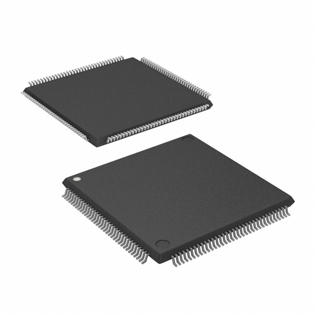
EP1K30QI208-2
| Part Description |
ACEX-1K® Field Programmable Gate Array (FPGA) IC 147 24576 1728 208-BFQFP |
|---|---|
| Quantity | 461 Available (as of June 15, 2026) |

| Product Category | Field Programmable Gate Array (FPGA) |
|---|---|
| Manufacturer | Intel |
| Manufacturing Status | Obsolete |
| Manufacturer Standard Lead Time | Contact Us |
| Datasheet |
Specifications & Environmental
| Device Package | 208-PQFP (28x28) | Grade | Industrial | Operating Temperature | 0°C – 70°C | ||
|---|---|---|---|---|---|---|---|
| Package / Case | 208-BFQFP | Number of I/O | 147 | Voltage | 2.375 V - 2.625 V | ||
| Mounting Method | Surface Mount | RoHS Compliance | RoHS non-compliant | REACH Compliance | REACH Unaffected | ||
| Moisture Sensitivity Level | 3 (168 Hours) | Number of LABs/CLBs | 216 | Number of Logic Elements/Cells | 1728 | ||
| Number of Gates | 119000 | ECCN | 3A991D | HTS Code | 8542.39.0001 | ||
| Qualification | N/A | Total RAM Bits | 24576 |
Overview of EP1K30QI208-2 – ACEX-1K® Field Programmable Gate Array (FPGA) IC 147 24576 1728 208-BFQFP
The EP1K30QI208-2 is an ACEX-1K family FPGA from Intel designed for system-on-a-programmable-chip (SOPC) integration. It combines mid-density programmable logic with embedded memory and flexible I/O to support functions such as on-chip memory, specialized logic, and dual-port embedded-array implementations.
Targeted at industrial and communications-oriented designs, this device delivers a balance of logic capacity, on-chip RAM, and I/O count in a compact surface-mount package for volume-focused and cost-sensitive applications.
Key Features
- Core Logic — Approximately 1,728 logic elements providing a programmable fabric sized for mid-density logic integration; device listing shows up to 119,000 system gates.
- Embedded Memory (EABs) — Total on-chip RAM of 24,576 bits with embedded array blocks (EABs) and dual-port capability to support efficient on-chip storage and megafunctions.
- I/O Flexibility — 147 user I/O pins with MultiVolt I/O capability (I/O can drive or be driven by 2.5-V, 3.3-V, or 5.0-V devices according to the device family specification) and programmable output options for interface adaptability.
- Supply and Operating Range — Operates with a 2.5-V internal supply and a specified voltage-supply range of 2.375 V to 2.625 V; rated for industrial operating temperatures from 0 °C to 70 °C.
- Configuration and Test — Built-in JTAG boundary-scan (IEEE 1149.1) for board test and support for in-circuit reconfigurability via external configuration devices or the JTAG port.
- Clocking and Timing — Built-in low-skew clock distribution trees with multiple global clocks and options such as ClockLock and ClockBoost for reduced clock delay and skew (family-level features).
- Interconnect and Arithmetic — FastTrack interconnect architecture with dedicated carry and cascade chains to implement arithmetic and high-fan-in logic functions efficiently.
- Package and Mounting — Surface-mount 208-pin BFQFP package (supplier package: 208-PQFP 28×28) for compact board integration.
Typical Applications
- Embedded Systems / SOPC Integration — Implement memory-backed megafunctions and custom logic for system integration on a single programmable device.
- Communications Equipment — Mid-density logic and embedded RAM support protocol processing and buffering demands in communications modules.
- Industrial Control — Programmable control, I/O interfacing, and local data buffering in industrial automation applications within the specified operating temperature range.
- Cost-Sensitive High-Volume Designs — Cost-optimized programmable architecture suitable for designs where integration and unit-cost are primary considerations.
Unique Advantages
- Balanced Integration: Combines 1,728 logic elements with 24,576 bits of on-chip RAM to reduce external component count and simplify board-level memory requirements.
- Flexible Interfacing: A large complement of 147 I/O pins with family-level MultiVolt I/O support simplifies interfacing to a variety of voltage domains.
- Deterministic Clocking: Low-skew clock distribution and multiple global clocks with ClockLock/ClockBoost options support predictable timing in synchronous designs.
- Test and Reconfiguration: Integrated JTAG boundary-scan and in-circuit reconfigurability enable board-level testability and field updates without additional logic consumption.
- Board-Level Friendly Package: 208-pin BFQFP surface-mount package (208-PQFP, 28×28) fits compact PCB layouts while preserving ample I/O.
- Industrial-Rated Operation: Supplied in an industrial grade variant with an operating range of 0 °C to 70 °C and defined supply voltage window for predictable deployment.
Why Choose EP1K30QI208-2?
The EP1K30QI208-2 delivers a mid-density ACEX-1K FPGA option that balances programmable logic capacity, embedded RAM, and I/O count in a compact surface-mount package. Its combination of approximately 1,728 logic elements, 24,576 bits of on-chip memory, and 147 user I/Os makes it well suited to SOPC integration, communications subsystems, and industrial control applications where integration and predictable behavior matter.
Supported by the ACEX-1K family feature set—on-chip EABs, JTAG boundary-scan, flexible clocking, and software design support from family development tools—this device provides a pragmatic, cost-conscious path to implement custom logic and embedded functions in volume designs.
Request a quote or submit an inquiry for pricing and availability of EP1K30QI208-2 to evaluate fit for your next design.


Date Founded: 1968
Headquarters: Santa Clara, California, USA
Employees: 130,000+
Revenue: $54.23 Billion
Certifications and Memberships: ISO9001:2015, ISO14001:2015, ISO17025:2017, ISO27001:2022, ISO45001:2018, ISO50001:2018


