
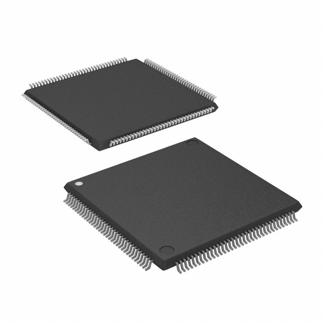
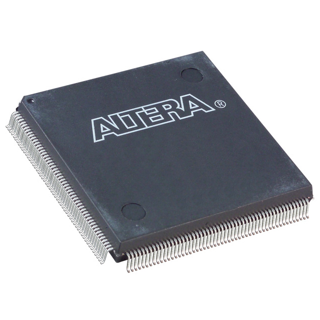
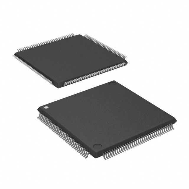
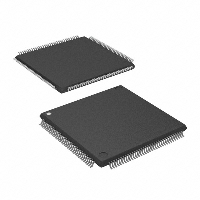
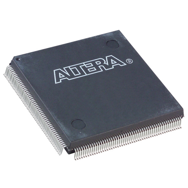
EP1K30TC144-1
| Part Description |
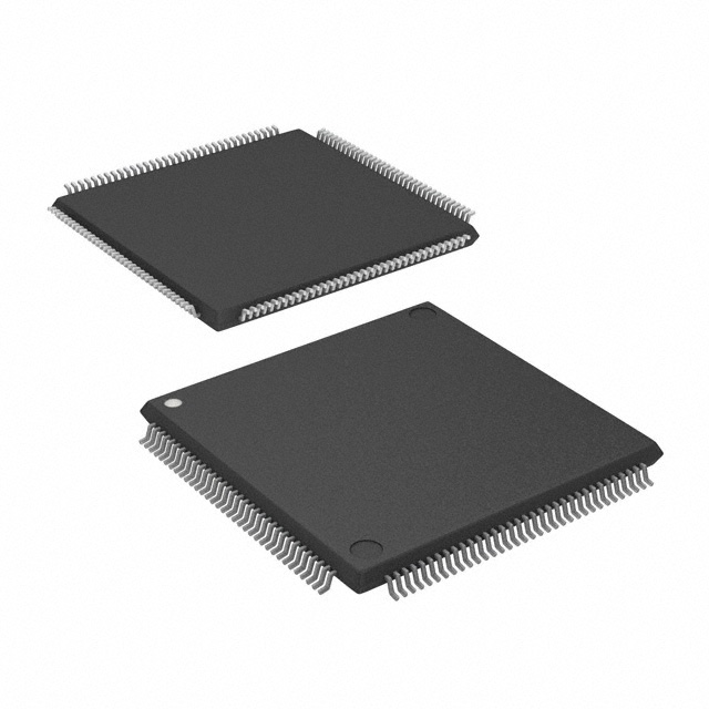
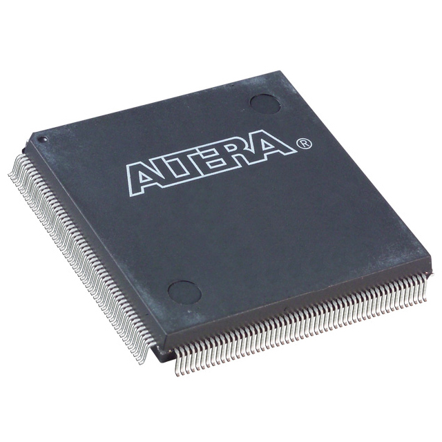
ACEX-1K® Field Programmable Gate Array (FPGA) IC 102 24576 1728 144-LQFP |
|---|---|
| Quantity | 90 Available (as of October 7, 2026) |
| Product Category | Field Programmable Gate Array (FPGA) |
|---|---|
| Manufacturer | Intel |
| Manufacturing Status | Obsolete |
| Manufacturer Standard Lead Time | Contact Us |
| Datasheet |
Specifications & Environmental
| Device Package | 144-TQFP (20x20) | Grade | Commercial | Operating Temperature | 0°C – 70°C | ||
|---|---|---|---|---|---|---|---|
| Package / Case | 144-LQFP | Number of I/O | 102 | Voltage | 2.375 V - 2.625 V | ||
| Mounting Method | Surface Mount | RoHS Compliance | RoHS non-compliant | REACH Compliance | REACH Unaffected | ||
| Moisture Sensitivity Level | 3 (168 Hours) | Number of LABs/CLBs | 216 | Number of Logic Elements/Cells | 1728 | ||
| Number of Gates | 119000 | ECCN | 3A991D | HTS Code | 8542.39.0001 | ||
| Qualification | N/A | Total RAM Bits | 24576 |
Overview of EP1K30TC144-1 – ACEX-1K FPGA, 1,728 logic elements, 24,576-bit embedded RAM, 102 I/Os, 144-LQFP
The EP1K30TC144-1 is an ACEX-1K family field programmable gate array (FPGA) from Intel, offering a compact, cost-efficient programmable logic solution in a 144-LQFP surface-mount package. It combines a 1,728‑logic‑element fabric with approximately 24,576 bits of embedded RAM and 102 user I/O pins, positioning it for system-on-a-programmable-chip (SOPC) integration and high-volume communications or control applications that require flexible I/O and embedded memory.
Key Features
- Core Logic — 1,728 logic elements providing combinational and registered logic for glue logic, control, and custom functions; equivalent to 119,000 maximum system gates for complex designs.
- Embedded Memory (EABs) — Approximately 24,576 bits of on-chip RAM organized in embedded array blocks suitable for FIFOs, small buffers, and storage of state data.
- I/O Capability — 102 user I/O pins in a 144‑lead LQFP package with MultiVolt I/O support for mixed-voltage interfacing (family feature), enabling direct interfacing to different logic levels.
- Package & Mounting — 144‑LQFP surface‑mount package (supplier device package listed as 144‑TQFP 20×20), enabling compact board layouts and automated assembly.
- Power & Voltage — Device operates with an internal 2.5‑V supply and a specified external supply range of 2.375 V to 2.625 V, supporting efficient power delivery for embedded applications.
- Operating Range — Commercial temperature grade with an operating range of 0 °C to 70 °C, suitable for a wide range of consumer and commercial electronic products.
- Clocking & Performance — Family features include built-in low‑skew clock distribution, options for reduced clock delay and skew, and bidirectional I/O performance up to 250 MHz (per family datasheet).
- Configuration & Test — In‑circuit reconfigurability via external configuration devices, intelligent controllers, or JTAG; includes IEEE 1149.1 (JTAG) boundary-scan support for board-level test.
- Compliance & Environmental — RoHS compliant; family-level features include PCI Local Bus Specification compatibility for -1 speed grade devices (as documented in the ACEX-1K datasheet).
Typical Applications
- System-on-a-Programmable-Chip (SOPC) — Integrate control logic, glue logic, and small embedded functions into a single device to reduce bill of materials and board complexity.
- Communications Interfaces — Implement protocol bridging, buffering, and custom I/O handling where embedded RAM and multiple I/O standards are needed.
- Embedded Control — Use as a programmable controller for motor drives, sensor aggregation, or custom state machines in commercial equipment.
- Prototyping and Logic Acceleration — Rapidly prototype custom digital blocks and offload timing-critical functions from microcontrollers or DSPs.
Unique Advantages
- Balanced integration: Combines 1,728 logic elements with embedded RAM to consolidate discrete logic and small memory functions into one package, reducing component count.
- Flexible I/O: 102 user I/Os and family support for multi-voltage signaling simplify interfacing with diverse peripherals and legacy logic levels.
- Compact package: 144‑lead LQFP surface‑mount packaging offers a compact footprint for space‑constrained boards while supporting automated assembly.
- Design and test support: Built‑in JTAG boundary-scan and support for in‑circuit reconfigurability streamline board bring‑up and manufacturing test flows.
- Predictable timing infrastructure: Low‑skew clock trees and dedicated carry/cascade chains (family features) enable more efficient implementation of arithmetic and high‑fan‑in logic.
- Regulated supply range: Narrow external supply window (2.375–2.625 V) and 2.5‑V internal supply simplify power‑supply design and decoupling strategies.
Why Choose EP1K30TC144-1?
The EP1K30TC144-1 is positioned as a cost-effective, compact FPGA for designers needing a blend of logic density, embedded memory, and flexible I/O in a commercial temperature grade. Its 1,728 logic elements and approximately 24,576 bits of embedded RAM allow efficient implementation of SOPC-style functions, buffering, and custom interfaces without large, power-hungry devices.
Backed by the ACEX-1K family design ecosystem and built‑in configuration and test features, this device suits engineering teams targeting high-volume or space-constrained applications that require reliable, reconfigurable logic with a clear upgrade path within the ACEX-1K family.
Request a quote or submit an inquiry to receive pricing and availability information for the EP1K30TC144-1.





















Date Founded: 1968
Headquarters: Santa Clara, California, USA
Employees: 130,000+
Revenue: $54.23 Billion
Certifications and Memberships: ISO9001:2015, ISO14001:2015, ISO17025:2017, ISO27001:2022, ISO45001:2018, ISO50001:2018


