
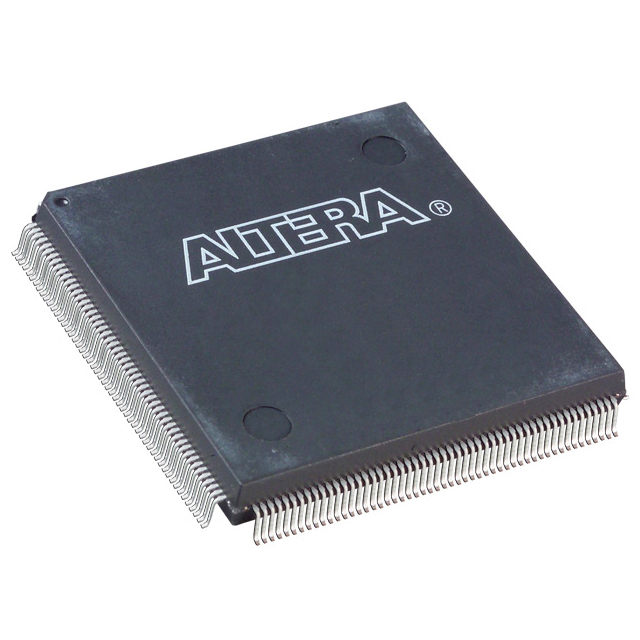
EP1K30QC208-2
| Part Description |
ACEX-1K® Field Programmable Gate Array (FPGA) IC 147 24576 1728 208-BFQFP |
|---|---|
| Quantity | 415 Available (as of June 15, 2026) |
| Product Category | Field Programmable Gate Array (FPGA) |
|---|---|
| Manufacturer | Intel |
| Manufacturing Status | Obsolete |
| Manufacturer Standard Lead Time | Contact Us |
| Datasheet |
Specifications & Environmental
| Device Package | 208-PQFP (28x28) | Grade | Commercial | Operating Temperature | 0°C – 70°C | ||
|---|---|---|---|---|---|---|---|
| Package / Case | 208-BFQFP | Number of I/O | 147 | Voltage | 2.375 V - 2.625 V | ||
| Mounting Method | Surface Mount | RoHS Compliance | RoHS non-compliant | REACH Compliance | REACH Unaffected | ||
| Moisture Sensitivity Level | 3 (168 Hours) | Number of LABs/CLBs | 216 | Number of Logic Elements/Cells | 1728 | ||
| Number of Gates | 119000 | ECCN | 3A991D | HTS Code | 8542.39.0001 | ||
| Qualification | N/A | Total RAM Bits | 24576 |
Overview of EP1K30QC208-2 – ACEX-1K® Field Programmable Gate Array (FPGA) IC 147 24576 1728 208-BFQFP
The EP1K30QC208-2 is an ACEX-1K programmable logic device optimized for system-on-a-programmable-chip integration. It combines a logic array with embedded memory blocks to implement a mix of general logic and megafunctions in a single surface-mount package.
Designed for cost-sensitive, high-density applications such as communications and embedded systems, this device provides 1,728 logic elements, 24,576 bits of on-chip RAM, dual-port embedded array capability, and flexible I/O behavior to support mixed-voltage interfaces.
Key Features
- Core Logic 1,728 logic elements and a maximum system gate count of 119,000 provide programmable capacity for medium-density designs.
- Embedded Memory 24,576 bits of total RAM with multiple embedded array blocks (EABs) supporting dual-port operation and up to 16-bit widths per block for efficient on-chip storage.
- I/O and Voltage MultiVolt I/O capability described in the ACEX-1K family supports interfacing with 2.5-V, 3.3-V, or 5.0-V devices while the device core supply is specified at 2.375 V to 2.625 V.
- Package & Mounting 208-BFQFP package (supplier device package: 208-PQFP, 28×28) with surface-mount mounting for standard PCB assembly.
- System Features Built-in JTAG boundary-scan (IEEE 1149.1) and in-circuit reconfigurability via external configuration devices or the JTAG port enable testability and field updates without consuming device logic.
- Clock and Performance Options Family features include low-skew clock distribution with options such as ClockLock and ClockBoost for reduced clock delay and controlled clock behavior.
- Routing & Arithmetic Support FastTrack interconnect, dedicated carry chains for arithmetic, and cascade chains for high fan-in logic support efficient implementation of adders, counters, and wide logic functions.
- Environmental & Operating Range Commercial-grade device with operating temperature 0 °C to 70 °C and RoHS compliance.
Typical Applications
- Communications Equipment Medium-density logic and embedded RAM make the device suitable for protocol handling, interface bridging, and packet-processing functions in communications designs.
- Embedded Controllers On-chip RAM and dual-port EABs enable local buffering and state machines for embedded control and coordination tasks.
- System Integration & SOPC Programmable logic plus embedded arrays support system-on-a-programmable-chip integration to consolidate multiple discrete components into a single device.
- Prototyping and Proof-of-Concept Reconfigurability and JTAG access facilitate iterative development and board-level testing of custom logic functions.
Unique Advantages
- Balanced Logic and Memory: 1,728 logic elements combined with 24,576 bits of RAM allow implementation of both control logic and local data storage without external memory in many designs.
- Flexible I/O Voltage Support: MultiVolt I/O capability enables direct interfacing with a range of external devices while maintaining a dedicated core supply range.
- Field Reconfigurability: In-circuit reconfigurability via external configuration devices or JTAG simplifies updates and iterative design changes without hardware replacement.
- Testability Built In: IEEE 1149.1 JTAG boundary-scan support is available without consuming user logic, aiding board-level test and diagnostics.
- Dedicated Arithmetic and Routing Resources: Carry and cascade chains plus FastTrack interconnect reduce design effort and improve predictable timing for arithmetic and wide logic functions.
- Surface-Mount, Standard Package: 208-pin PQFP/BFQFP package supports established PCB assembly flows and compact board layouts.
Why Choose EP1K30QC208-2?
The EP1K30QC208-2 positions itself as a versatile, commercial-grade programmable logic device for designers needing a balanced combination of logic elements and embedded RAM in a compact surface-mount package. Its family-level features—such as MultiVolt I/O, in-circuit reconfigurability, and dedicated arithmetic resources—help simplify system integration while preserving flexibility during development and deployment.
This device is well suited to teams building communications equipment, embedded controllers, and SOPC solutions that require moderate logic density, on-chip memory, and board-level testability, backed by the ACEX-1K family feature set documented in the product datasheet.
Request a quote or submit an inquiry for pricing and availability of EP1K30QC208-2 to get technical details and lead-time information tailored to your project needs.


Date Founded: 1968
Headquarters: Santa Clara, California, USA
Employees: 130,000+
Revenue: $54.23 Billion
Certifications and Memberships: ISO9001:2015, ISO14001:2015, ISO17025:2017, ISO27001:2022, ISO45001:2018, ISO50001:2018


