
EP1K30FI256-2N
| Part Description |
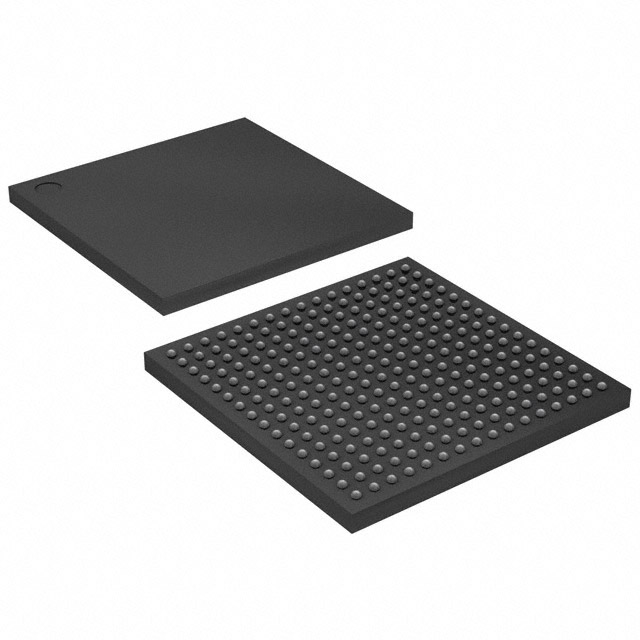
ACEX-1K® Field Programmable Gate Array (FPGA) IC 171 24576 1728 256-BGA |
|---|---|
| Quantity | 135 Available (as of October 7, 2026) |
| Product Category | Field Programmable Gate Array (FPGA) |
|---|---|
| Manufacturer | Intel |
| Manufacturing Status | Obsolete |
| Manufacturer Standard Lead Time | Contact Us |
| Datasheet |
Specifications & Environmental
| Device Package | 256-FBGA (17x17) | Grade | Industrial | Operating Temperature | -40°C – 85°C | ||
|---|---|---|---|---|---|---|---|
| Package / Case | 256-BGA | Number of I/O | 171 | Voltage | 2.375 V - 2.625 V | ||
| Mounting Method | Surface Mount | RoHS Compliance | Unknown | REACH Compliance | REACH Unaffected | ||
| Moisture Sensitivity Level | 3 (168 Hours) | Number of LABs/CLBs | 216 | Number of Logic Elements/Cells | 1728 | ||
| Number of Gates | 119000 | ECCN | 3A991D | HTS Code | 8542.39.0001 | ||
| Qualification | N/A | Total RAM Bits | 24576 |
Overview of EP1K30FI256-2N – ACEX-1K Field Programmable Gate Array (FPGA), 1,728 LEs, 24,576-bit RAM, 171 I/O, 256-BGA
The EP1K30FI256-2N is an Intel ACEX-1K family FPGA providing a programmable logic fabric with embedded memory and flexible I/O in a 256-ball fine-pitch BGA package. Built for industrial applications, this device delivers 1,728 logic elements, 24,576 bits of on-chip RAM and up to 171 user I/O pins for system-on-a-programmable-chip integration and moderate-density logic designs.
Its architecture includes embedded array blocks for efficient memory and specialized logic, on-chip clock distribution and dedicated arithmetic/cascade chains—features that suit communications, embedded control, and system integration use cases that require reconfigurability and compact implementation.
Key Features
- Logic Capacity — 1,728 logic elements (LEs) supporting up to 119,000 gates for moderate-density programmable logic implementations.
- Embedded Memory — 24,576 total RAM bits implemented with embedded array blocks (EABs), including dual-port capability and up to 16-bit width per EAB for efficient on-chip storage and memory-intensive megafunctions.
- I/O and Voltage — Up to 171 user I/O pins with MultiVolt I/O support described by the ACEX-1K family; device operates with an internal 2.5-V supply and specified supply range of 2.375 V to 2.625 V.
- Package & Mounting — 256-ball FineLine BGA (256-FBGA, 17×17) in a surface-mount package suitable for compact board designs.
- Temperature & Grade — Industrial grade operation with an operating temperature range of −40 °C to 85 °C for deployment in industrial environments.
- Clocking & Performance — Built-in low-skew clock distribution trees with options such as ClockLock and ClockBoost to reduce clock delay and skew; up to six global clock signals and four global clear signals on the family.
- Dedicated Arithmetic & Routing — Dedicated carry and cascade chains for efficient implementation of adders, counters and high-fan-in logic; FastTrack continuous routing for predictable interconnect delays.
- Testability & Reconfiguration — JTAG boundary-scan (IEEE 1149.1) for in-system test and in-circuit reconfigurability via external configuration devices, intelligent controller, or JTAG.
- Power & I/O Control — Programmable output slew-rate control, open-drain option, clamp-to-VCCIO selection and per-pin tri-state enable for optimized signal integrity and interface flexibility.
Typical Applications
- Communications Equipment — Implement protocol logic, packet buffering and specialized functions that benefit from embedded memory and moderate gate density.
- Embedded Control & Motor Drive — Use on-chip logic and dedicated arithmetic chains for control algorithms, counters and deterministic timing in industrial controllers.
- System Integration / SOPC — Consolidate multiple functions into a single programmable device using embedded RAM and logic to reduce board-level BOM and simplify integration.
- Interface & I/O Bridging — Leverage flexible I/O and voltage-domain support to bridge different logic families and manage mixed-voltage interfaces.
Unique Advantages
- Balanced Logic and Memory: Combines 1,728 logic elements with 24,576 bits of embedded RAM to implement both combinational logic and on-chip storage without excessive external memory.
- Flexible I/O Management: Up to 171 user I/O pins with per-pin control of slew rate, tri-state and clamp options for robust interfacing to diverse peripherals and bus standards.
- Industrial Temperature Range: Specified for −40 °C to 85 °C operation, making the device suitable for many industrial deployments.
- Efficient Arithmetic and High-Fan-In Logic: Dedicated carry and cascade chains accelerate adders, counters and complex logic structures while simplifying synthesis and place-and-route.
- In-System Test and Reconfiguration: Built-in JTAG boundary-scan and in-circuit reconfigurability options support convenient board-level test and field updates.
- Compact, Board-Friendly Package: 256-FBGA (17×17) surface-mount package enables compact PCB designs and same-frame pin migration across FineLine BGA options.
Why Choose EP1K30FI256-2N?
The EP1K30FI256-2N is positioned for engineers who need a compact, industrial-grade FPGA with a balanced mix of logic, embedded memory and flexible I/O in a fine-pitch BGA package. Its combination of 1,728 logic elements, 24,576 bits of RAM and 171 I/O pins delivers a practical platform for communications, embedded control and system integration tasks that require on-chip memory and deterministic logic structures.
With industry-oriented temperature rating, built-in JTAG testability, dedicated arithmetic chains and clocking options, this device provides a reliable, reconfigurable building block for medium-density designs that benefit from a single-chip programmable solution.
Request a quote or submit a quotation request to obtain pricing, availability and ordering information for EP1K30FI256-2N. Our team can provide lead-time details and support for integrating this ACEX-1K device into your designs.
























Date Founded: 1968
Headquarters: Santa Clara, California, USA
Employees: 130,000+
Revenue: $54.23 Billion
Certifications and Memberships: ISO9001:2015, ISO14001:2015, ISO17025:2017, ISO27001:2022, ISO45001:2018, ISO50001:2018


