
EP1K30FC256-3
| Part Description |
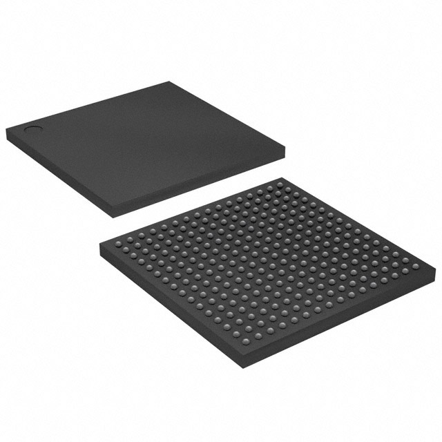
ACEX-1K® Field Programmable Gate Array (FPGA) IC 171 24576 1728 256-BGA |
|---|---|
| Quantity | 1,425 Available (as of June 10, 2026) |

| Product Category | Field Programmable Gate Array (FPGA) |
|---|---|
| Manufacturer | Intel |
| Manufacturing Status | Obsolete |
| Manufacturer Standard Lead Time | Contact Us |
| Datasheet |
Specifications & Environmental
| Device Package | 256-FBGA (17x17) | Grade | Commercial | Operating Temperature | 0°C – 70°C | ||
|---|---|---|---|---|---|---|---|
| Package / Case | 256-BGA | Number of I/O | 171 | Voltage | 2.375 V - 2.625 V | ||
| Mounting Method | Surface Mount | RoHS Compliance | RoHS non-compliant | REACH Compliance | REACH Unaffected | ||
| Moisture Sensitivity Level | 3 (168 Hours) | Number of LABs/CLBs | 216 | Number of Logic Elements/Cells | 1728 | ||
| Number of Gates | 119000 | ECCN | 3A991D | HTS Code | 8542.39.0001 | ||
| Qualification | N/A | Total RAM Bits | 24576 |
Overview of EP1K30FC256-3 – ACEX-1K® Field Programmable Gate Array (FPGA) IC 171 24576 1728 256-BGA
The EP1K30FC256-3 is an ACEX 1K family programmable logic device from Intel, delivering 1,728 logic elements, 24,576 bits of embedded RAM and up to 171 user I/O pins in a 256-ball FineLine BGA (17×17) surface-mount package. It targets designs that require moderate logic density combined with embedded memory and flexible I/O for system-level integration.
Built for commercial-grade applications, the device supports in-circuit reconfigurability and family-level features for memory-intensive and communications-focused designs, while operating from a 2.375 V to 2.625 V supply and across a 0 °C to 70 °C temperature range.
Key Features
- Programmable Logic Core — 1,728 logic elements and a maximum device gate count of 119,000 provide configurable logic capacity for a wide range of functions.
- Embedded Memory — 24,576 total RAM bits across embedded array blocks (EABs) enable efficient implementation of on-chip buffers, FIFOs and small memory structures.
- I/O and Voltage Flexibility — Up to 171 user I/O pins with MultiVolt I/O capability (family-level feature) to interface with 2.5 V, 3.3 V or 5.0 V devices.
- Package and Mounting — 256-FBGA (17×17) surface-mount package delivers a compact footprint for board-level implementations.
- Configuration and Test — Supports in-circuit reconfigurability and JTAG boundary-scan (BST) for programming and board-level test without consuming core logic resources.
- Power and Timing — Operates from a 2.375 V to 2.625 V supply; family documentation highlights low power consumption and built-in clock distribution features for predictable timing.
- Commercial Grade and Compliance — Specified for 0 °C to 70 °C operation and RoHS-compliant.
Typical Applications
- Communications Equipment — Implement protocol processing, buffering and custom packet-handling logic using the device's embedded RAM and logic resources.
- System-on-a-Programmable-Chip (SOPC) — Integrate specialized logic functions and memory on a single device to reduce board-level complexity.
- Interface Bridging and I/O Expansion — Use the MultiVolt-capable I/O and 171 pins for level translation, bus interfacing and peripheral bridging.
- Memory and Buffering — Leverage dual-port-capable EABs for small on-chip buffers, FIFOs and shared memory structures.
Unique Advantages
- High integration in a compact package: 1,728 logic elements and 24,576 RAM bits in a 256-FBGA reduce BOM and board space compared with discrete solutions.
- Flexible I/O support: Up to 171 user I/O pins and MultiVolt I/O enable direct interfacing to multiple bus voltages without external level shifters.
- Designed for system integration: Embedded array blocks with dual-port capability simplify implementation of memory-heavy functions and megafunctions.
- Production and testability: Family-level JTAG boundary-scan and 100% functional testing in manufacturing aid board-level bring-up and diagnostics.
- Commercial-grade reliability: Specified operating range of 0 °C to 70 °C and RoHS compliance make the part suitable for standard commercial applications.
- Path for migration: ACEX 1K family package options and documented pin-compatibility support device migration within the family.
Why Choose EP1K30FC256-3?
The EP1K30FC256-3 combines a balanced mix of logic capacity, embedded memory and flexible I/O in a compact 256-FBGA package, making it well suited for communications, SOPC integration and board-level interface tasks in commercial applications. Its family-level features—such as in-circuit reconfigurability, JTAG boundary-scan, and embedded array blocks—help streamline development and reduce system complexity.
Designers benefit from documented tool support and automatic place-and-route workflows provided for the ACEX 1K family, along with tested manufacturing quality and RoHS compliance. The part is a practical choice for teams needing a moderately dense, memory-capable programmable device with commercial operating specifications.
Request a quote or submit an RFQ to obtain pricing and availability for the EP1K30FC256-3.


Date Founded: 1968
Headquarters: Santa Clara, California, USA
Employees: 130,000+
Revenue: $54.23 Billion
Certifications and Memberships: ISO9001:2015, ISO14001:2015, ISO17025:2017, ISO27001:2022, ISO45001:2018, ISO50001:2018


