
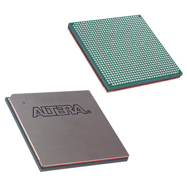
EP1S25F1020C7
| Part Description |
Stratix® Field Programmable Gate Array (FPGA) IC 706 1944576 25660 1020-BBGA |
|---|---|
| Quantity | 909 Available (as of June 15, 2026) |

| Product Category | Field Programmable Gate Array (FPGA) |
|---|---|
| Manufacturer | Intel |
| Manufacturing Status | Obsolete |
| Manufacturer Standard Lead Time | Contact Us |
| Datasheet |
Specifications & Environmental
| Device Package | 1020-FBGA (33x33) | Grade | Commercial | Operating Temperature | 0°C – 85°C | ||
|---|---|---|---|---|---|---|---|
| Package / Case | 1020-BBGA | Number of I/O | 706 | Voltage | 1.425 V - 1.575 V | ||
| Mounting Method | Surface Mount | RoHS Compliance | RoHS non-compliant | REACH Compliance | REACH Unaffected | ||
| Moisture Sensitivity Level | 3 (168 Hours) | Number of LABs/CLBs | 2566 | Number of Logic Elements/Cells | 25660 | ||
| Number of Gates | N/A | ECCN | 3A001A7A | HTS Code | 8542.39.0001 | ||
| Qualification | N/A | Total RAM Bits | 1944576 |
Overview of EP1S25F1020C7 – Stratix Field Programmable Gate Array (FPGA), 1020-BBGA
The EP1S25F1020C7 is a Stratix® FPGA from Intel provided in a 1020-BBGA (1020-FBGA, 33×33) surface-mount package. This commercial-grade device offers 25,660 logic elements, approximately 1.94 Mbits of on-chip RAM (1,944,576 bits), and 706 general-purpose I/O pins, making it suited to designs that require substantial logic capacity and high I/O density.
Architecturally, the device aligns with the Stratix family feature set described in the Stratix Device Handbook, including TriMatrix memory structures, dedicated DSP block interfaces, PLLs and clock networks, double-data-rate I/O support, and configuration and debug features such as JTAG boundary-scan and SignalTap II. Electrical and environmental parameters include a core supply window of 1.425 V to 1.575 V and an operating temperature range of 0 °C to 85 °C; the device is RoHS compliant.
Key Features
- Logic Capacity – 25,660 logic elements for implementing complex combinational and sequential logic.
- Embedded Memory – Approximately 1.94 Mbits (1,944,576 bits) of on-chip RAM for data buffering, FIFOs, and local storage.
- I/O Density – 706 I/O pins to support high-pin-count interfaces and multi-channel connectivity.
- Package & Mounting – Supplied in a 1020-BBGA (supplier package 1020-FBGA, 33×33) surface-mount package suitable for compact board layouts.
- Power Supply – Core voltage range of 1.425 V to 1.575 V to match standard Stratix supply domains.
- Operating Conditions – Commercial-grade device rated for 0 °C to 85 °C operation.
- Clocking & DSP Support – Device family documentation describes PLLs, enhanced/fast PLL options, and DSP block interfaces for clock management and arithmetic acceleration.
- I/O & Interface Capabilities – Stratix architecture coverage includes double-data-rate I/O and advanced I/O standards support as documented in the device handbook.
- Configuration & Debug – Family features include JTAG boundary-scan, SignalTap II embedded logic analyzer, and multiple configuration schemes including partial reconfiguration and SEU detection features as described in the device documentation.
- Compliance – RoHS compliant.
Typical Applications
- High-density digital logic and prototyping – Use the FPGA's 25,660 logic elements and embedded memory to implement complex control, protocol, and custom logic blocks for system prototyping and development.
- High-pin-count interface systems – Leverage 706 I/O pins for multi-channel data acquisition, board-level bridging, or systems requiring broad external connectivity.
- Signal processing and DSP functions – Deploy DSP block interfaces and on-chip memory for data path processing, filtering, and arithmetic-heavy functions.
- Custom embedded memory designs – Approximately 1.94 Mbits of on-chip RAM provides local storage for buffering, packet handling, and low-latency data manipulation.
Unique Advantages
- Substantial logic resources: 25,660 logic elements provide headroom for complex logic integration and multi-function designs.
- Large I/O complement: 706 I/O pins enable high-density external interfacing without extensive external glue logic.
- Significant on-chip memory: Approximately 1.94 Mbits of embedded RAM reduces reliance on external memory for many buffering and FIFO needs.
- Documented Stratix architecture: Family-level documentation details clocking networks, DSP interfaces, memory architectures, and configuration/debugging tools to support design implementation.
- Commercial-grade readiness: Surface-mount 1020-BBGA package, defined operating temperature range (0 °C to 85 °C), and RoHS compliance simplify integration into commercial product lines.
- Flexible power domain: Defined core supply window (1.425 V–1.575 V) supports predictable power planning and regulator selection.
Why Choose EP1S25F1020C7?
The EP1S25F1020C7 delivers a balanced combination of logic density, embedded memory, and high I/O count in a compact 1020-BBGA package for commercial embedded designs. It is well suited to teams implementing substantial custom logic, multi-channel interfaces, or DSP-accelerated data paths who require a documented Stratix architecture and on-board resources to reduce external component count.
Backed by the Stratix device documentation and design guidance from the device handbook, EP1S25F1020C7 is intended for projects where predictable electrical characteristics (1.425 V–1.575 V supply, 0 °C–85 °C operating range) and RoHS compliance are required. Specify this part when your design needs a high-capacity, commercially graded FPGA with broad I/O and embedded memory.
Request a quote or submit an inquiry for pricing and availability for EP1S25F1020C7 to receive lead-time and procurement information.


Date Founded: 1968
Headquarters: Santa Clara, California, USA
Employees: 130,000+
Revenue: $54.23 Billion
Certifications and Memberships: ISO9001:2015, ISO14001:2015, ISO17025:2017, ISO27001:2022, ISO45001:2018, ISO50001:2018


