
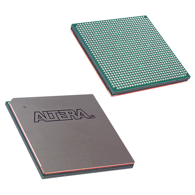
EP1S25F672C7
| Part Description |
Stratix® Field Programmable Gate Array (FPGA) IC 473 1944576 25660 672-BBGA |
|---|---|
| Quantity | 1,649 Available (as of June 10, 2026) |

| Product Category | Field Programmable Gate Array (FPGA) |
|---|---|
| Manufacturer | Intel |
| Manufacturing Status | Obsolete |
| Manufacturer Standard Lead Time | Contact Us |
| Datasheet |
Specifications & Environmental
| Device Package | 672-FBGA (27x27) | Grade | Commercial | Operating Temperature | 0°C – 85°C | ||
|---|---|---|---|---|---|---|---|
| Package / Case | 672-BBGA | Number of I/O | 473 | Voltage | 1.425 V - 1.575 V | ||
| Mounting Method | Surface Mount | RoHS Compliance | RoHS non-compliant | REACH Compliance | REACH Unaffected | ||
| Moisture Sensitivity Level | 3 (168 Hours) | Number of LABs/CLBs | 2566 | Number of Logic Elements/Cells | 25660 | ||
| Number of Gates | N/A | ECCN | 3A991D | HTS Code | 8542.39.0001 | ||
| Qualification | N/A | Total RAM Bits | 1944576 |
Overview of EP1S25F672C7 – Stratix® Field Programmable Gate Array, 672-BBGA
The EP1S25F672C7 is a Stratix® family Field Programmable Gate Array (FPGA) offered in a 672-ball BGA package. It combines a sizable logic fabric and on-chip memory with a large I/O count to address compute- and I/O-intensive designs.
Architecturally consistent with the Stratix device family, the device benefits from the series' documented features such as programmable clocking (PLLs), flexible I/O structures, embedded memory modes, DSP/multiplier resources, and standard configuration and test support. Typical market segments include communications, signal processing, and general-purpose embedded systems requiring commercial-grade operation.
Key Features
- Logic Capacity Provides 25,660 logic elements to implement complex combinational and sequential logic.
- Embedded Memory Approximately 1.94 Mbits of on-chip RAM to support buffering, FIFOs, and embedded data storage across diverse memory modes described for the Stratix family.
- I/O Density 473 I/O pins for broad external interfacing and high-pin-count designs.
- Clocking and DSP Support Built on the Stratix architecture that includes PLLs, clock networks, and dedicated multiplier/DSP block interfaces for deterministic clocking and arithmetic acceleration.
- I/O Features Series-level documentation includes high-speed differential I/O support, programmable drive strength, slew-rate control, and additional advanced I/O capabilities suitable for multi-standard interfacing.
- Package & Mounting 672-ball BGA package (Supplier Device Package: 672-FBGA, 27×27) with surface-mount mounting for board-level integration.
- Power & Voltage Core supply voltage range: 1.425 V to 1.575 V to support specified device operation.
- Commercial Temperature Grade Rated for operation from 0 °C to 85 °C, appropriate for commercial applications.
- Standards & Test Family-level features include IEEE 1149.1 JTAG boundary-scan and configuration/testing support as documented in the Stratix device handbook.
- Compliance RoHS compliant.
Typical Applications
- High-bandwidth Communications Large I/O count and series-level high-speed I/O capabilities enable interfaces and protocol handling for communications equipment.
- Signal Processing & DSP On-chip memory and Stratix-family DSP/multiplier interfaces support data-path acceleration, filtering, and real-time processing tasks.
- Embedded System Integration Substantial logic resources and configurable I/O make the device suitable for embedded control, protocol bridging, and custom peripheral integration.
- Memory Interfacing Documented external RAM interfacing modes in the Stratix family support designs that require external memory controllers or large buffers.
Unique Advantages
- Significant Logic Engine: 25,660 logic elements provide the capacity to implement complex finite-state machines, datapaths, and control logic within a single device.
- Embedded Memory for On-Chip Data Storage: Approximately 1.94 Mbits of on-chip RAM reduces dependence on external memory for many buffering and storage tasks.
- High I/O Count: 473 I/Os enable dense peripheral connections and multi-channel interfaces without immediate need for additional I/O expanders.
- Family-Level Clocking & DSP Features: Stratix documentation details PLLs, clock networks, and DSP block interfaces that support precise timing and arithmetic-intensive functions.
- Commercial-Grade Thermal Envelope: 0 °C to 85 °C operating range aligns with commercial product deployments and standard thermal design practices.
- RoHS Compliance: Meets RoHS requirements for environmentally conscious designs.
Why Choose EP1S25F672C7?
EP1S25F672C7 positions itself as a Stratix-family FPGA option for engineers who need a balanced combination of logic density, embedded memory, and extensive I/O in a commercial-grade BGA package. The device leverages the Stratix architecture elements documented in the device handbook—clocking, memory modes, DSP interfaces, and robust I/O capabilities—making it suitable for designs that require integrated compute and interface resources.
Supported by family-level configuration and test features, and supplied in a 672-ball FBGA package, this device is targeted at development and production systems where on-chip resources and a high pin count reduce system complexity and board-level component count.
Request a quote or submit an inquiry for pricing and availability of EP1S25F672C7 to receive lead-time and volume information tailored to your design requirements.


Date Founded: 1968
Headquarters: Santa Clara, California, USA
Employees: 130,000+
Revenue: $54.23 Billion
Certifications and Memberships: ISO9001:2015, ISO14001:2015, ISO17025:2017, ISO27001:2022, ISO45001:2018, ISO50001:2018


