
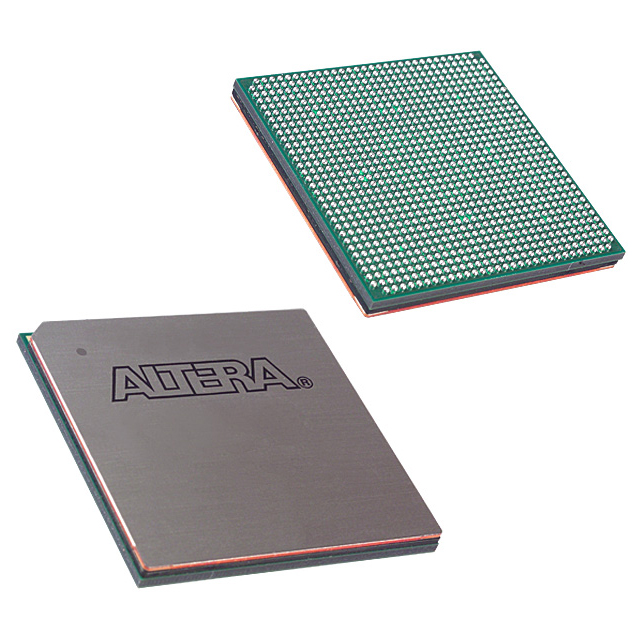
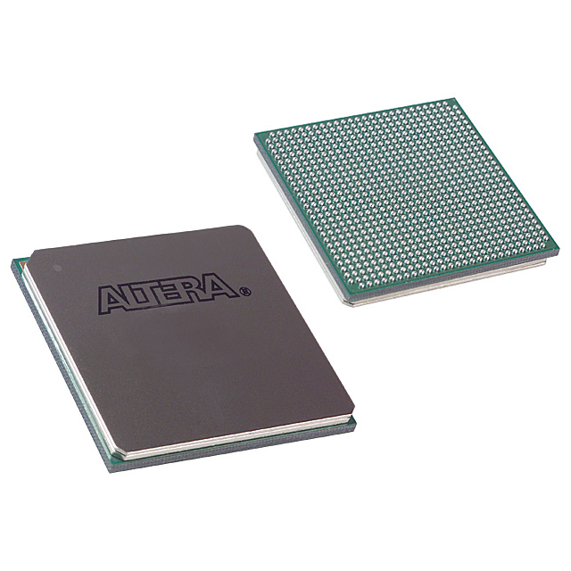
EP1S30F1020I6N
| Part Description |
Stratix® Field Programmable Gate Array (FPGA) IC 726 3317184 32470 1020-BBGA |
|---|---|
| Quantity | 917 Available (as of June 15, 2026) |

| Product Category | Field Programmable Gate Array (FPGA) |
|---|---|
| Manufacturer | Intel |
| Manufacturing Status | Obsolete |
| Manufacturer Standard Lead Time | Contact Us |
| Datasheet |
Specifications & Environmental
| Device Package | 1020-FBGA (33x33) | Grade | Industrial | Operating Temperature | -40°C – 100°C | ||
|---|---|---|---|---|---|---|---|
| Package / Case | 1020-BBGA | Number of I/O | 726 | Voltage | 1.425 V - 1.575 V | ||
| Mounting Method | Surface Mount | RoHS Compliance | Unknown | REACH Compliance | REACH Unaffected | ||
| Moisture Sensitivity Level | 3 (168 Hours) | Number of LABs/CLBs | 3247 | Number of Logic Elements/Cells | 32470 | ||
| Number of Gates | N/A | ECCN | 3A001A2A | HTS Code | 8542.39.0001 | ||
| Qualification | N/A | Total RAM Bits | 3317184 |
Overview of EP1S30F1020I6N – Stratix® Field Programmable Gate Array (FPGA) IC 726 3317184 32470 1020-BBGA
The EP1S30F1020I6N is a Stratix® FPGA from Intel delivered in a 1020-FBGA (33×33) surface-mount package. The device integrates 32,470 logic elements across 3,247 LABs and provides approximately 3.3 Mbits of embedded memory (3,317,184 bits) together with 726 I/O pins.
On-chip resources and architecture documented in the Stratix device handbook—including PLLs and clock networks, DSP/multiplier blocks, high-speed I/O features, and robust configuration/debug options—make this device appropriate for designs that require high logic and I/O density within an industrial temperature range.
Key Features
- Core Density 32,470 logic elements organized into 3,247 LABs provide high-density programmable logic for complex designs.
- Embedded Memory Approximately 3.3 Mbits of on-chip RAM (3,317,184 bits) supporting multiple memory modes and TriMatrix memory structures for flexible data storage and buffering.
- I/O Resources 726 I/O pins with support for advanced I/O capabilities noted in the device handbook, including double-data-rate I/O, programmable drive strength, differential on-chip termination, and high-speed differential interfaces.
- Clocking and DSP Integrated PLLs and hierarchical clock networks, enhanced and fast PLL options, plus dedicated DSP and multiplier blocks for signal processing and timing-critical functions.
- Configuration & Debug IEEE 1149.1 (JTAG) boundary-scan support, SignalTap II embedded logic analyzer, and multiple configuration schemes including partial and remote update modes as described in the device documentation.
- Package & Power Surface-mount 1020-FBGA (33×33) package; specified supply voltage range of 1.425 V to 1.575 V to match system power requirements.
- Temperature & Compliance Industrial-grade device with an operating temperature range of −40 °C to 100 °C and RoHS compliance for environmental requirements.
Typical Applications
- High-speed communications — Leverages the device’s high I/O count and high-speed differential I/O support for network interface logic and protocol bridging.
- Signal processing and DSP — On-chip DSP blocks and multiplier resources enable real-time data processing and algorithm acceleration.
- Memory interface and controllers — Embedded RAM plus documented external RAM interfacing modes support buffering, caching, and memory-controller implementations.
- Industrial control and automation — Industrial-grade temperature range and dense I/O make the device suitable for control logic, sensor aggregation, and machine I/O tasks.
Unique Advantages
- High logic and I/O density: 32,470 logic elements and 726 I/Os reduce the need for external glue logic and simplify integration of complex functions.
- Substantial on-chip memory: Approximately 3.3 Mbits of embedded RAM enables local buffering and reduces external memory bandwidth requirements.
- Flexible clocking and DSP resources: Integrated PLLs, hierarchical clocking, and dedicated DSP/multiplier blocks support timing-critical and signal-processing designs.
- Comprehensive configuration and debug: JTAG, SignalTap II, and partial configuration support facilitate development, testing, and field updates.
- Industrial temperature support: Rated for −40 °C to 100 °C, aligning with demanding environmental requirements for industrial applications.
- Standard surface-mount packaging: 1020-FBGA (33×33) offers a compact, manufacturable footprint for volume production.
Why Choose EP1S30F1020I6N?
The EP1S30F1020I6N combines a high logic element count, abundant on-chip memory, and a large I/O complement in a single industrial-grade Stratix FPGA package. Its documented architecture—including advanced I/O, clocking, DSP resources, and mature configuration/debug features—suits teams building complex embedded systems, high-speed interfaces, and industrial controllers who require a dense, configurable logic platform.
Backed by the Stratix device family documentation, the part provides a clear specification set for system design, allowing engineering and procurement teams to evaluate integration, thermal, and power requirements precisely.
Request a quote or submit an inquiry to receive pricing, availability, and additional technical support information for the EP1S30F1020I6N.


Date Founded: 1968
Headquarters: Santa Clara, California, USA
Employees: 130,000+
Revenue: $54.23 Billion
Certifications and Memberships: ISO9001:2015, ISO14001:2015, ISO17025:2017, ISO27001:2022, ISO45001:2018, ISO50001:2018


