
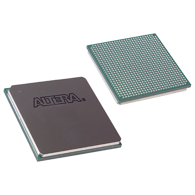
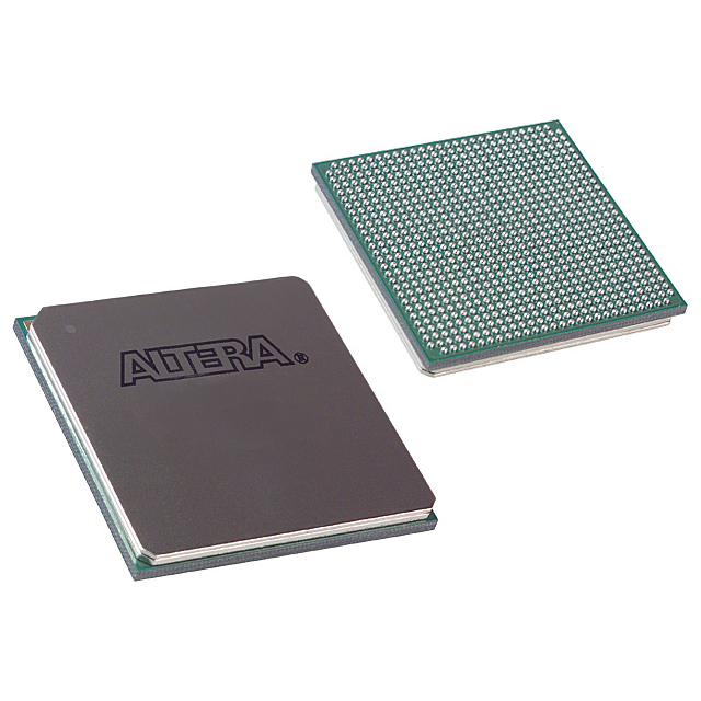
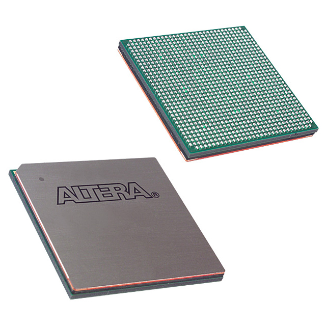
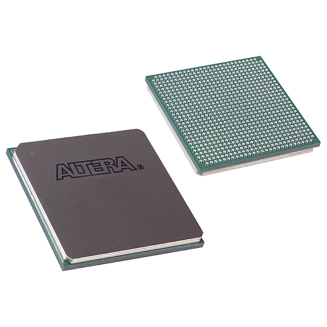
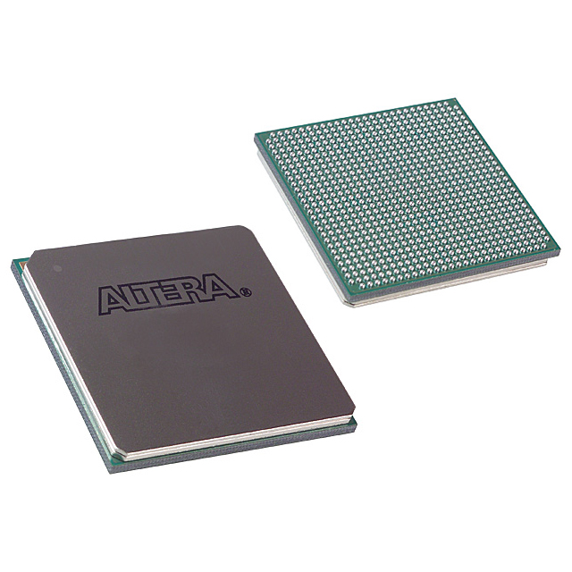
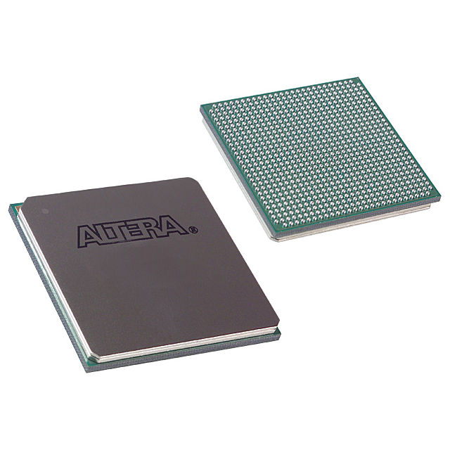
EP1S30F780C5N
| Part Description |
Stratix® Field Programmable Gate Array (FPGA) IC 597 3317184 32470 780-BBGA, FCBGA |
|---|---|
| Quantity | 678 Available (as of October 8, 2026) |
| Product Category | Field Programmable Gate Array (FPGA) |
|---|---|
| Manufacturer | Intel |
| Manufacturing Status | Obsolete |
| Manufacturer Standard Lead Time | Contact Us |
| Datasheet |
Specifications & Environmental
| Device Package | 780-FBGA (29x29) | Grade | Commercial | Operating Temperature | 0°C – 85°C | ||
|---|---|---|---|---|---|---|---|
| Package / Case | 780-BBGA, FCBGA | Number of I/O | 597 | Voltage | 1.425 V - 1.575 V | ||
| Mounting Method | Surface Mount | RoHS Compliance | Unknown | REACH Compliance | REACH Unaffected | ||
| Moisture Sensitivity Level | 3 (168 Hours) | Number of LABs/CLBs | 3247 | Number of Logic Elements/Cells | 32470 | ||
| Number of Gates | N/A | ECCN | 3A001A7A | HTS Code | 8542.39.0001 | ||
| Qualification | N/A | Total RAM Bits | 3317184 |
Overview of EP1S30F780C5N – Stratix® Field Programmable Gate Array (FPGA), 32,470 logic elements, ~3.317 Mbits RAM, 597 I/O, 780‑BBGA
The EP1S30F780C5N is a Stratix® family FPGA in a 780‑ball FCBGA package (29×29) optimized for board‑level designs requiring high logic density and extensive I/O. The device integrates approximately 32,470 logic elements and approximately 3.317 Mbits of embedded RAM with a 597‑pin I/O complement, providing a compact platform for complex digital designs.
Designed with Stratix architecture features documented in the device handbook—including programmable I/O, clocking resources and embedded memory—the device is targeted at commercial applications that require scalable logic, memory and interface capability within a Surface Mount package.
Key Features
- Core Logic Approximately 32,470 logic elements for implementing complex combinational and sequential logic functions.
- Embedded Memory Approximately 3.317 Mbits of on‑chip RAM (TriMatrix memory architecture referenced in the device handbook) for buffering, FIFOs and local storage.
- I/O Capability 597 I/O pins accessible from a 780‑ball FCBGA (29×29) package, supporting a broad range of external interfaces and high pin count designs.
- Clocking & Timing Stratix clock network features and PLL resources are documented for flexible clocking, hierarchical clock distribution and timing control.
- DSP & Arithmetic Resources Multiplier and DSP block interfaces are part of the Stratix architecture to support arithmetic‑intensive functions and signal processing datapaths.
- Configuration & Debug Device handbook sections describe JTAG boundary‑scan support and embedded logic analysis capability (SignalTap II) for configuration and in‑system debug.
- Power & Supply Core voltage supply range: 1.425 V to 1.575 V, enabling consistent power planning for board designs.
- Package & Mounting 780‑BBGA FCBGA surface‑mount package (supplier device package: 780‑FBGA, 29×29) for compact, high‑density PCB layouts.
- Operating Conditions & Compliance Commercial grade operation from 0 °C to 85 °C and RoHS compliant for standard commercial product deployments.
Typical Applications
- High‑performance networking and communications Implement protocol engines, packet processing and interface aggregation using the device's high logic density and abundant I/O.
- Signal processing and DSP Leverage embedded multipliers, DSP interfaces and on‑chip RAM for filtering, transforms and real‑time data paths.
- Memory interfacing and controllers Use the device's memory architecture and I/O resources for external RAM interfacing, buffering and custom memory controllers.
- Board‑level prototyping and system control Deploy as a central programmable device for integrating glue logic, custom peripherals and system control functions on commercial products.
Unique Advantages
- High logic density: Approximately 32,470 logic elements provide the capacity to implement complex state machines, datapaths and custom processors on a single device.
- Significant on‑chip memory: Approximately 3.317 Mbits of embedded RAM reduce external memory dependence and lower system latency for buffering and packet storage.
- Extensive I/O reach: 597 I/O pins in a 780‑ball FCBGA enable wide peripheral and interface connectivity without compromising PCB routing density.
- Flexible clocking and DSP support: Stratix clock networks, PLLs and multiplier/DSP resources support precise timing and arithmetic workloads essential for high‑throughput designs.
- Commercial temperature and RoHS compliance: Rated for 0 °C to 85 °C operation and RoHS compliant for standard commercial product lifecycles.
- Compact surface‑mount package: 780‑BBGA (29×29) package balances I/O count and board space for compact system designs.
Why Choose EP1S30F780C5N?
The EP1S30F780C5N delivers a balanced combination of logic density, embedded memory and I/O capacity within a compact 780‑ball FCBGA package. It is suitable for commercial designs that require integrated DSP resources, flexible clocking and substantial on‑chip RAM while maintaining standard commercial temperature and RoHS compliance.
This device is well suited for engineers and teams working on communications, signal processing, memory interfacing or board‑level system control applications who need a programmable, high‑capacity FPGA foundation backed by the Stratix device architecture and its documented features.
Request a quote or submit a procurement inquiry to receive pricing and availability for the EP1S30F780C5N for your next design.





















Date Founded: 1968
Headquarters: Santa Clara, California, USA
Employees: 130,000+
Revenue: $54.23 Billion
Certifications and Memberships: ISO9001:2015, ISO14001:2015, ISO17025:2017, ISO27001:2022, ISO45001:2018, ISO50001:2018


