
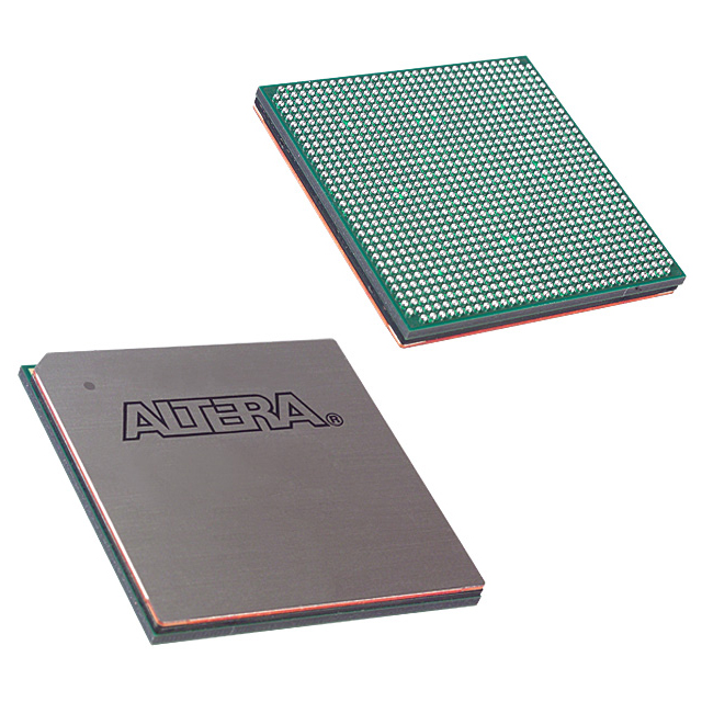
EP1S30F780C6N
| Part Description |
Stratix® Field Programmable Gate Array (FPGA) IC 597 3317184 32470 780-BBGA, FCBGA |
|---|---|
| Quantity | 324 Available (as of June 14, 2026) |

| Product Category | Field Programmable Gate Array (FPGA) |
|---|---|
| Manufacturer | Intel |
| Manufacturing Status | Obsolete |
| Manufacturer Standard Lead Time | Contact Us |
| Datasheet |
Specifications & Environmental
| Device Package | 780-FBGA (29x29) | Grade | Commercial | Operating Temperature | 0°C – 85°C | ||
|---|---|---|---|---|---|---|---|
| Package / Case | 780-BBGA, FCBGA | Number of I/O | 597 | Voltage | 1.425 V - 1.575 V | ||
| Mounting Method | Surface Mount | RoHS Compliance | Unknown | REACH Compliance | REACH Unaffected | ||
| Moisture Sensitivity Level | 3 (168 Hours) | Number of LABs/CLBs | 3247 | Number of Logic Elements/Cells | 32470 | ||
| Number of Gates | N/A | ECCN | 3A001A7A | HTS Code | 8542.39.0001 | ||
| Qualification | N/A | Total RAM Bits | 3317184 |
Overview of EP1S30F780C6N – Stratix® Field Programmable Gate Array, 780‑FBGA (29×29)
The EP1S30F780C6N is an Intel Stratix® Field Programmable Gate Array (FPGA) supplied in a 780‑ball FCBGA package. It delivers a large logic fabric and on‑chip memory with extensive I/O connectivity for complex digital designs.
Targeted at commercial applications, this device combines approximately 32,470 logic elements, roughly 3.32 Mbits of embedded memory, and 597 I/O pins to support high‑density logic, memory interfacing, and high‑speed I/O subsystems.
Key Features
- Logic Capacity – Approximately 32,470 logic elements to implement complex logic, control and datapath functions.
- On‑Chip Memory – Approximately 3.32 Mbits of embedded RAM suitable for buffering, FIFOs and local storage.
- I/O Density – 597 I/O pins to support wide parallel interfaces, memory buses and multiple high‑speed links.
- Clocking and Timing – Stratix device architecture includes PLLs and clock network features described in the Stratix Device Handbook for flexible clock distribution and phase control.
- High‑Speed I/O Support – Device family documentation includes support for DDR I/O modes, advanced I/O standards and differential on‑chip termination to simplify high‑speed interface design.
- Configuration & Test – Stratix family configuration and testing features include JTAG boundary‑scan and support for partial reconfiguration workflows as documented in the device handbook.
- Power and Supply – Operates from a core supply range of 1.425 V to 1.575 V to match system power rails and design margins.
- Package & Mounting – Surface mount 780‑BBGA (supplier package: 780‑FBGA, 29×29) for high‑density board integration.
- Commercial Temperature Grade – Rated for operation from 0 °C to 85 °C for standard commercial environments.
- RoHS Compliant – Meets RoHS requirements for reduced hazardous substances.
Typical Applications
- High‑performance digital signal processing – Use the device’s large logic capacity and on‑chip memory for DSP blocks, filtering, and real‑time signal manipulation.
- High‑speed interface bridging – 597 I/O pins and Stratix family high‑speed I/O features support wide memory buses, DDR interfaces, and multi‑lane link implementations.
- Prototyping and system integration – Reconfigurable logic and standard configuration/test features such as JTAG make the device suitable for board‑level prototyping and iterative development.
- Custom control and glue logic – Large logic element count enables integration of complex control engines, protocol translators, and peripheral aggregation on a single device.
Unique Advantages
- High integration density: Approximately 32,470 logic elements and ~3.32 Mbits of embedded RAM reduce the need for external ASICs and discrete memories, simplifying BOM and board layout.
- Extensive I/O capability: 597 I/O pins provide the flexibility to implement wide parallel interfaces, multiple memory channels or many peripheral connections without additional I/O expanders.
- Flexible clocking: Stratix device clocking and PLL features enable precise clock management for complex multi‑clock designs and high‑speed interfaces.
- Commercial temperature suitability: Rated 0 °C to 85 °C for deployment in mainstream commercial systems where standard operating temperature coverage is required.
- Package for dense boards: 780‑FBGA (29×29) surface‑mount package supports compact, high‑density PCB designs while delivering large I/O counts.
- Standards‑aligned development: On‑device support for JTAG and documented family features for configuration and partial reconfiguration streamline development and test workflows.
Why Choose EP1S30F780C6N?
The EP1S30F780C6N offers a balance of significant logic resources, on‑chip memory, and high I/O density in a single surface‑mount 780‑FBGA package. It is well suited to designers who need to consolidate complex digital functions, high‑speed interfaces and memory buffering into a single FPGA for commercial applications.
Backed by the Stratix device family documentation and Intel’s device architecture, this part provides the architectural building blocks—large logic capacity, embedded memory, flexible clocking and robust I/O—that enable scalable, maintainable system designs.
Request a quote or submit a purchase inquiry today to confirm pricing and availability for EP1S30F780C6N and to discuss lead times and volume options.


Date Founded: 1968
Headquarters: Santa Clara, California, USA
Employees: 130,000+
Revenue: $54.23 Billion
Certifications and Memberships: ISO9001:2015, ISO14001:2015, ISO17025:2017, ISO27001:2022, ISO45001:2018, ISO50001:2018


