
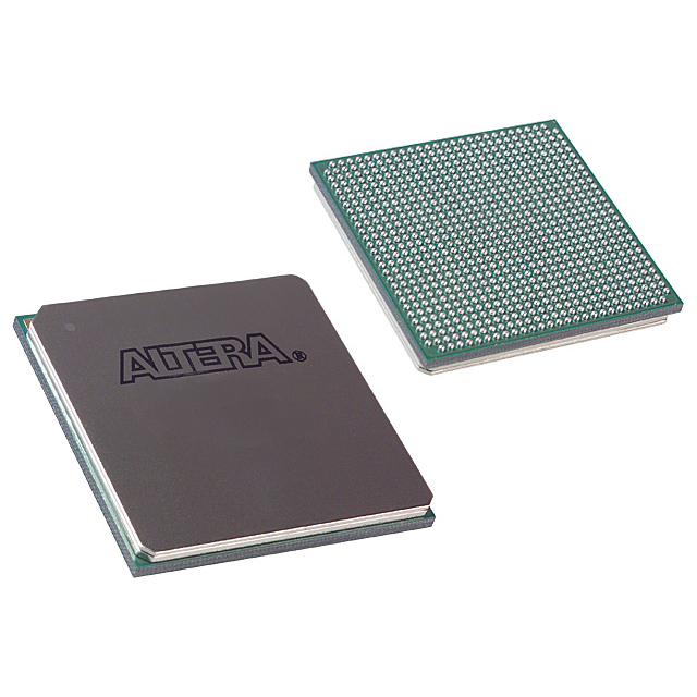
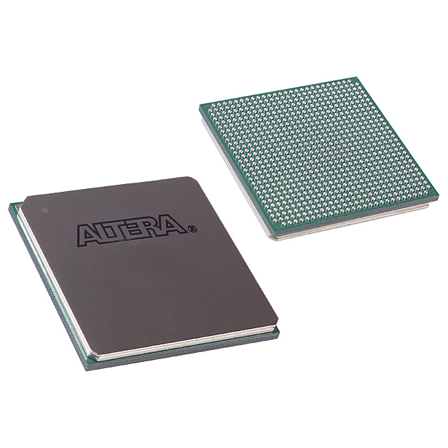
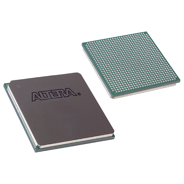
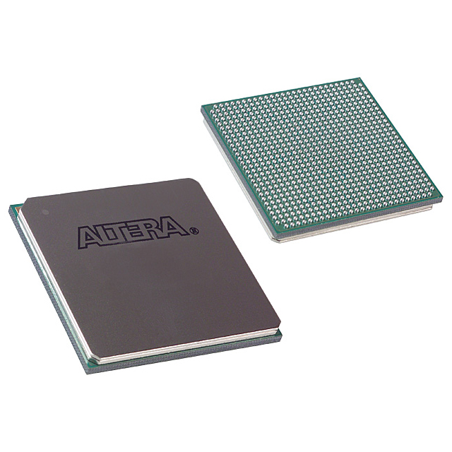
EP1S30F780C7N
| Part Description |
Stratix® Field Programmable Gate Array (FPGA) IC 597 3317184 32470 780-BBGA, FCBGA |
|---|---|
| Quantity | 887 Available (as of October 7, 2026) |
| Product Category | Field Programmable Gate Array (FPGA) |
|---|---|
| Manufacturer | Intel |
| Manufacturing Status | Obsolete |
| Manufacturer Standard Lead Time | Contact Us |
| Datasheet |
Specifications & Environmental
| Device Package | 780-FBGA (29x29) | Grade | Commercial | Operating Temperature | 0°C – 85°C | ||
|---|---|---|---|---|---|---|---|
| Package / Case | 780-BBGA, FCBGA | Number of I/O | 597 | Voltage | 1.425 V - 1.575 V | ||
| Mounting Method | Surface Mount | RoHS Compliance | Unknown | REACH Compliance | REACH Unaffected | ||
| Moisture Sensitivity Level | 3 (168 Hours) | Number of LABs/CLBs | 3247 | Number of Logic Elements/Cells | 32470 | ||
| Number of Gates | N/A | ECCN | 3A001A7A | HTS Code | 8542.39.0001 | ||
| Qualification | N/A | Total RAM Bits | 3317184 |
Overview of EP1S30F780C7N – Stratix® Field Programmable Gate Array (FPGA), 780‑FBGA
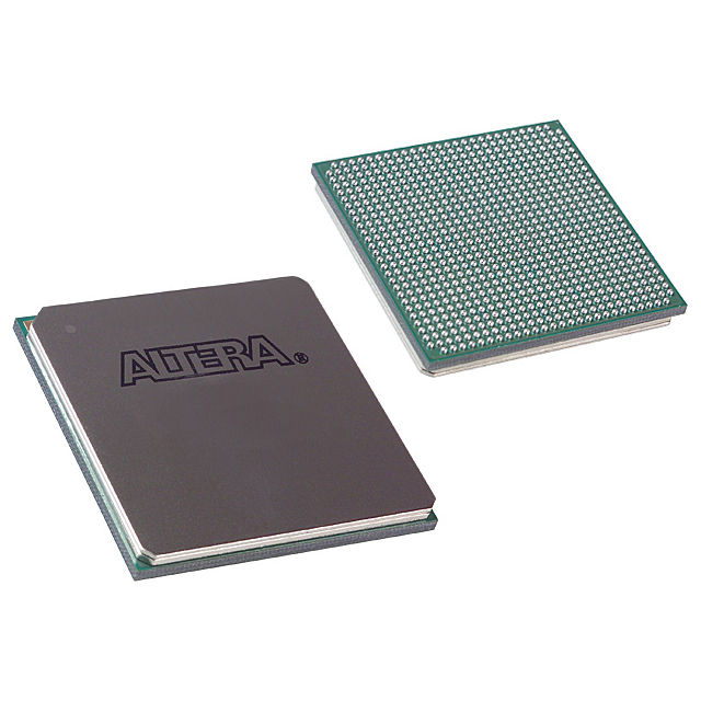
The EP1S30F780C7N is a Stratix® Field Programmable Gate Array (FPGA) IC from Intel (Altera), offered in a 780‑ball FCBGA package. It provides a programmable fabric based on the Stratix device architecture and is intended for commercial‑grade embedded and digital logic applications.
With 32,470 logic elements, on‑chip embedded memory and a high I/O count, the device is suited for designs that require dense logic integration, flexible I/O connectivity, and on‑chip memory resources within a surface‑mount FCBGA package.
Key Features
- Logic Capacity — 32,470 logic elements (LEs) for implementing complex digital functions and custom logic.
- Embedded Memory — Approximately 3.32 Mbits of on‑chip RAM (3,317,184 total RAM bits) for buffering, FIFOs, and local storage.
- I/O Resources — 597 user I/O pins to support dense external interfacing and multi‑lane connectivity.
- Stratix Architecture (documented) — Device handbook content for the Stratix family describes architecture elements such as Logic Array Blocks, TriMatrix memory, multiplier blocks, DSP block interfaces, and advanced I/O structures to guide system integration.
- Clocking & PLLs — The device documentation includes PLLs and hierarchical clocking schemes for advanced timing and clock distribution strategies.
- Configuration & Test Support — Datasheet material covers configuration modes, JTAG boundary‑scan support and embedded logic analysis features for development and production testing.
- Package & Mounting — 780‑BBGA FCBGA package (supplier package noted as 780‑FBGA, 29×29) designed for surface‑mount PCB assembly.
- Power & Operating Range — Core supply voltage range of 1.425 V to 1.575 V and commercial operating temperature range of 0 °C to 85 °C.
- Compliance — RoHS compliant and delivered in a commercial grade classification.
Typical Applications
- Communications Infrastructure — Programmable logic and abundant I/O allow implementation of custom protocol engines, data path processing and interface bridging.
- Digital Signal Processing — On‑chip RAM and documented multiplier/DSP block interfaces support FIR filters, FFT stages and stream processing pipelines.
- Embedded System Prototyping — Dense logic resources and flexible configuration options make the device suitable for prototyping custom SoC functions and hardware accelerators.
- High‑Density I/O Control — Large I/O count supports board‑level aggregation, multi‑lane IO, and complex peripheral interfacing in compact packages.
Unique Advantages
- Substantial Logic Density: 32,470 logic elements enable consolidation of multiple functions into a single FPGA, reducing BOM and board complexity.
- Significant Embedded Memory: Approximately 3.32 Mbits of on‑chip RAM provides local storage for buffering and state, reducing reliance on external memory.
- High I/O Count: 597 I/O pins allow flexible interfacing to peripherals, transceivers and parallel data channels without extensive external bridging.
- Documented Stratix Architecture: Comprehensive device handbook material covering LEs, memory modes, PLLs, I/O features and configuration options helps accelerate design and integration.
- Commercial Temperature & RoHS Compliance: Rated for 0 °C to 85 °C operation and RoHS compliant for broad commercial applications and standard manufacturing flows.
- FCBGA Packaging for Dense Boards: 780‑FBGA (29×29) package supports high pin density in space‑constrained layouts while enabling surface‑mount assembly.
Why Choose EP1S30F780C7N?
The EP1S30F780C7N positions itself as a Stratix family FPGA option that balances sizable logic resources, multi‑megabit embedded memory, and a high I/O count within a compact 780‑ball FCBGA package. It is suitable for commercial designs that require integrated digital processing, flexible I/O connectivity and established Stratix documentation for architecture and integration guidance.
Design teams targeting embedded DSP, protocol handling or custom logic consolidation will find the EP1S30F780C7N offers a measurable combination of capacity and package density backed by device handbook content from the Stratix family to support implementation and testing.
Request a quote or submit an inquiry to obtain pricing, lead‑time and availability for the EP1S30F780C7N.
























Date Founded: 1968
Headquarters: Santa Clara, California, USA
Employees: 130,000+
Revenue: $54.23 Billion
Certifications and Memberships: ISO9001:2015, ISO14001:2015, ISO17025:2017, ISO27001:2022, ISO45001:2018, ISO50001:2018


