
EP1S40F780C8
| Part Description |
Stratix® Field Programmable Gate Array (FPGA) IC 615 3423744 41250 780-BBGA, FCBGA |
|---|---|
| Quantity | 1,464 Available (as of June 10, 2026) |

| Product Category | Field Programmable Gate Array (FPGA) |
|---|---|
| Manufacturer | Intel |
| Manufacturing Status | Obsolete |
| Manufacturer Standard Lead Time | Contact Us |
| Datasheet |
Specifications & Environmental
| Device Package | 780-FBGA (29x29) | Grade | Commercial | Operating Temperature | 0°C – 85°C | ||
|---|---|---|---|---|---|---|---|
| Package / Case | 780-BBGA, FCBGA | Number of I/O | 615 | Voltage | 1.425 V - 1.575 V | ||
| Mounting Method | Surface Mount | RoHS Compliance | RoHS non-compliant | REACH Compliance | REACH Unaffected | ||
| Moisture Sensitivity Level | 3 (168 Hours) | Number of LABs/CLBs | 4125 | Number of Logic Elements/Cells | 41250 | ||
| Number of Gates | N/A | ECCN | 3A001A7A | HTS Code | 8542.39.0001 | ||
| Qualification | N/A | Total RAM Bits | 3423744 |
Overview of EP1S40F780C8 – Stratix® FPGA, 41,250 logic elements, 780-FBGA
The EP1S40F780C8 is a Stratix® field programmable gate array (FPGA) by Intel (Altera) delivered in a 780-ball FCBGA package. It provides a high-density programmable fabric with 41,250 logic elements and approximately 3.42 Mbits of embedded memory for complex digital designs.
With 615 user I/O pins, on-chip clocking and DSP resources described in the Stratix device handbook, and a 1.425 V–1.575 V core supply window, this FPGA targets designs that require dense logic, substantial embedded memory, and extensive external interfacing within commercial temperature ranges.
Key Features
- Logic Capacity Provides 41,250 logic elements suitable for implementing complex state machines, datapaths, and custom logic functions.
- Embedded Memory Approximately 3.42 Mbits of on-chip RAM to support buffers, FIFOs, and local storage for data-intensive functions.
- High I/O Count 615 user I/O pins enable dense external connectivity for multi-channel interfaces and parallel buses.
- Clocking and DSP Resources Architecture details in the Stratix device handbook describe PLLs, clock networks, multiplier blocks, and DSP block interfaces for synchronous and arithmetic-intensive designs.
- Configuration & Debug Supports industry-standard configuration and testing features documented in the Stratix handbook, including JTAG boundary-scan and SignalTap II embedded logic analysis, plus multiple configuration schemes and partial reconfiguration options.
- Power Supply Core voltage specified between 1.425 V and 1.575 V for predictable power planning and supply design.
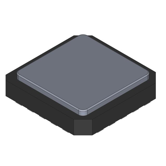
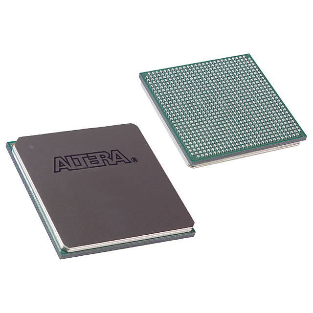
- Package & Mounting 780-ball BGA (FCBGA) package, supplier device package listed as 780-FBGA (29×29); surface-mount mounting for board-level integration.
- Environmental & Grade Commercial-grade device with an operating temperature range of 0 °C to 85 °C and RoHS compliance.
Typical Applications
- High-density digital processing Implement complex finite-state machines and custom datapaths using the 41,250 logic elements and on-chip RAM.
- Multi-channel I/O systems Leverage 615 I/O pins for dense parallel interfaces, protocol bridging, and multi-lane capture/drive applications.
- Embedded memory buffering Use approximately 3.42 Mbits of embedded memory for packet buffering, frame storage, and local data manipulation.
- Timing- and clock-sensitive designs Employ the device’s documented PLLs and clock networks to manage complex clock domains and synchronous data paths.
Unique Advantages
- High integration density: Consolidates substantial logic and memory on a single device to reduce board-level component count and simplify system architecture.
- Extensive external connectivity: 615 I/O pins allow high-pin-count interfaces without external multiplexing, supporting richer system integration.
- Flexible configuration and debug: Built-in support for JTAG boundary-scan and SignalTap II (per the Stratix handbook) accelerates bring-up and in-system debugging.
- Documented architecture and tooling: Coverage in the Stratix device handbook details architecture blocks such as TriMatrix memory, multiplier blocks, PLLs, and configuration modes to aid design planning.
- Commercial-grade and RoHS compliant: Designed for commercial temperature operation (0 °C to 85 °C) and compliant with RoHS requirements for global manufacturability.
Why Choose EP1S40F780C8?
The EP1S40F780C8 delivers a balance of logic capacity, embedded memory, and high I/O count in a compact 780-ball FCBGA package, making it suitable for commercial designs that demand dense programmable logic and extensive external interfacing. Its documented Stratix architecture—covering clocking, DSP, memory modes, and configuration—helps shorten development time and supports complex system requirements.
This device is appropriate for design teams building high-density digital systems, multi-interface controllers, and memory-buffered datapaths who need a commercially graded FPGA backed by comprehensive device documentation and configuration features.
Request a quote or submit an inquiry to receive pricing, lead-time, and availability for the EP1S40F780C8. Our team will respond with the specific purchasing and technical information you need.


Date Founded: 1968
Headquarters: Santa Clara, California, USA
Employees: 130,000+
Revenue: $54.23 Billion
Certifications and Memberships: ISO9001:2015, ISO14001:2015, ISO17025:2017, ISO27001:2022, ISO45001:2018, ISO50001:2018


