
EP1S40F780I6
| Part Description |
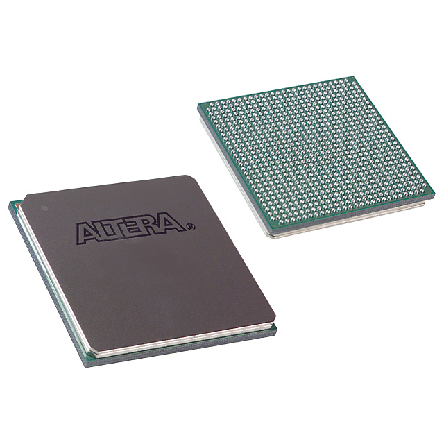
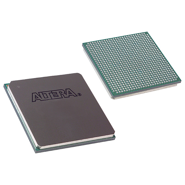
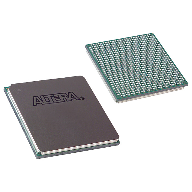
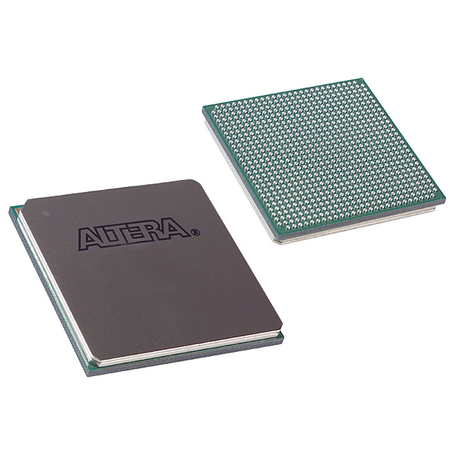
Stratix® Field Programmable Gate Array (FPGA) IC 615 3423744 41250 780-BBGA, FCBGA |
|---|---|
| Quantity | 130 Available (as of October 8, 2026) |

| Product Category | Field Programmable Gate Array (FPGA) |
|---|---|
| Manufacturer | Intel |
| Manufacturing Status | Obsolete |
| Manufacturer Standard Lead Time | Contact Us |
| Datasheet |
Specifications & Environmental
| Device Package | 780-FBGA (29x29) | Grade | Industrial | Operating Temperature | -40°C – 100°C | ||
|---|---|---|---|---|---|---|---|
| Package / Case | 780-BBGA, FCBGA | Number of I/O | 615 | Voltage | 1.425 V - 1.575 V | ||
| Mounting Method | Surface Mount | RoHS Compliance | Unknown | REACH Compliance | REACH Unaffected | ||
| Moisture Sensitivity Level | 3 (168 Hours) | Number of LABs/CLBs | 4125 | Number of Logic Elements/Cells | 41250 | ||
| Number of Gates | N/A | ECCN | 3A001A7A | HTS Code | 8542.39.0001 | ||
| Qualification | N/A | Total RAM Bits | 3423744 |
Overview of EP1S40F780I6 – Stratix® Field Programmable Gate Array (FPGA) IC 615 3423744 41250 780-BBGA, FCBGA
The EP1S40F780I6 is a Stratix-series Field Programmable Gate Array optimized for high-density logic and extensive I/O connectivity. It implements the Stratix architecture described in the Stratix Device Handbook, providing a combination of core logic, embedded memory, and advanced I/O and clocking resources.
Designed for industrial-grade applications, this device delivers 41,250 logic elements, approximately 3.42 Mbits of embedded RAM, and 615 I/O pins in a 780-ball FCBGA package, making it suitable for designs that require substantial on-chip resources and robust operating temperature range.
Key Features
- Core Logic 41,250 logic elements organized across 4,125 LABs for implementing complex custom logic and state machines.
- Embedded Memory Approximately 3.42 Mbits of on-chip RAM to support buffering, packet processing, and local data storage.
- I/O Capacity 615 I/O pins to support wide parallel buses, multi-channel interfaces, and extensive board-level connectivity.
- Clocking and DSP Support Stratix architecture includes integrated PLLs and dedicated DSP block interfaces as described in the device handbook, enabling flexible clock networks and signal-processing datapaths.
- Advanced I/O Features Device documentation covers high-speed differential I/O support and DDR I/O modes, useful for external RAM interfacing and high-speed links.
- Configuration and Test Support for standard configuration and boundary-scan (JTAG) methods along with on-chip logic analysis and configuration options referenced in the handbook.
- Package and Mounting 780-ball BGA (780-FBGA, 29×29) surface-mount package for compact board integration and high pin count routing.
- Power and Temperature Core voltage range 1.425 V to 1.575 V and industrial operating temperature range of −40 °C to 100 °C for use in temperature-variable environments.
- Regulatory Status RoHS-compliant manufacturing.
Typical Applications
- High-speed memory interfaces Use the device's on-chip RAM and documented external RAM interfacing capabilities to implement memory controllers and buffer-intensive applications.
- Signal processing and DSP Leverage the Stratix DSP block interfaces and abundant logic elements for custom filters, transforms, and real-time data processing engines.
- Multi-channel I/O systems Deploy the 615 I/O pins and advanced I/O features for multi-lane data acquisition, protocol bridging, or wide parallel peripheral interfaces.
- Prototyping and system glue logic Implement complex control logic, protocol conversion, and system-level integration using the large logic and memory resources.
Unique Advantages
- High logic density: 41,250 logic elements provide the capacity to consolidate multiple functions into a single device, reducing board-level BOM and interconnect complexity.
- Substantial embedded RAM: Approximately 3.42 Mbits of on-chip memory supports local buffering and high-throughput data paths without immediate reliance on external memory.
- Extensive I/O footprint: 615 I/O pins accommodate complex interfacing requirements and enable flexible partitioning of signals across the PCB.
- Industrial temperature rating: Rated for −40 °C to 100 °C operation to meet the needs of equipment deployed in temperature-variable environments.
- Flexible clocking and DSP support: Integrated PLLs and DSP block interfaces described in the device documentation enable versatile clock architectures and signal-processing implementations.
- Compact, high-density package: 780-ball FCBGA (29×29) package provides high pin count in a compact footprint for space-constrained designs.
Why Choose EP1S40F780I6?
The EP1S40F780I6 delivers a balanced combination of logic density, on-chip memory, and extensive I/O in an industrial-grade Stratix FPGA package. It is well-suited for designers who need to integrate substantial custom logic, implement high-throughput data paths, or consolidate multiple board-level functions into a single programmable device.
As part of the Stratix family, this device is documented in the Stratix Device Handbook, which details architecture elements such as logic array blocks, memory modes, clock networks, and configuration options—useful resources for planning scalable, long-lived designs.
Request a quote or submit an inquiry to receive pricing and availability information for the EP1S40F780I6. Include your quantity and delivery needs to expedite the response.
























Date Founded: 1968
Headquarters: Santa Clara, California, USA
Employees: 130,000+
Revenue: $54.23 Billion
Certifications and Memberships: ISO9001:2015, ISO14001:2015, ISO17025:2017, ISO27001:2022, ISO45001:2018, ISO50001:2018


