
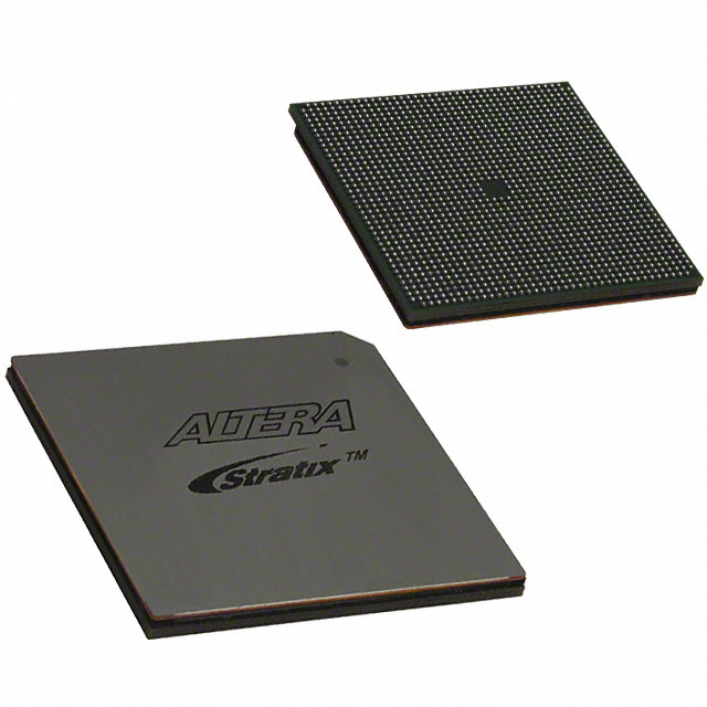
EP1S80F1508C7
| Part Description |
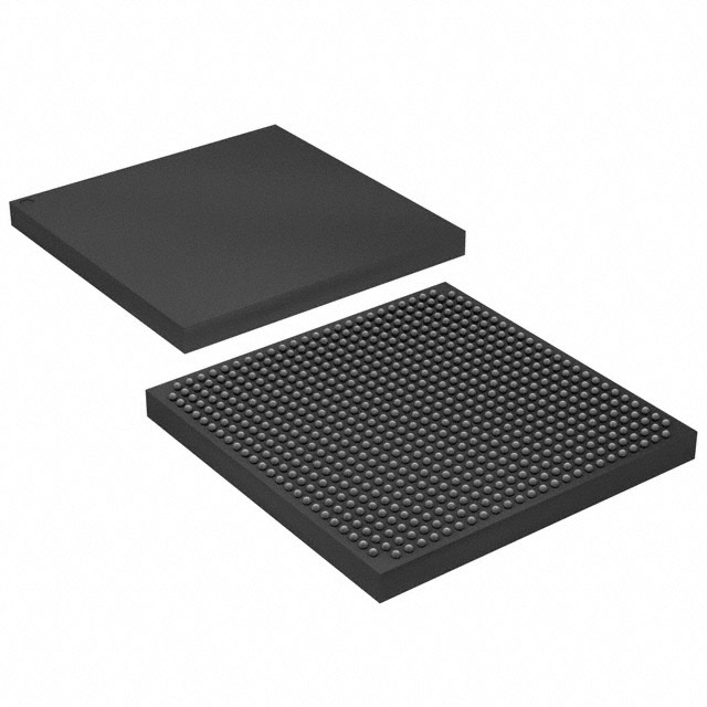
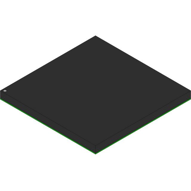
Stratix® Field Programmable Gate Array (FPGA) IC 1203 7427520 79040 1508-BBGA, FCBGA |
|---|---|
| Quantity | 211 Available (as of June 14, 2026) |

| Product Category | Field Programmable Gate Array (FPGA) |
|---|---|
| Manufacturer | Intel |
| Manufacturing Status | Obsolete |
| Manufacturer Standard Lead Time | Contact Us |
| Datasheet |
Specifications & Environmental
| Device Package | 1508-FBGA, FC (40x40) | Grade | Commercial | Operating Temperature | 0°C – 85°C | ||
|---|---|---|---|---|---|---|---|
| Package / Case | 1508-BBGA, FCBGA | Number of I/O | 1203 | Voltage | 1.425 V - 1.575 V | ||
| Mounting Method | Surface Mount | RoHS Compliance | RoHS non-compliant | REACH Compliance | REACH Unaffected | ||
| Moisture Sensitivity Level | 3 (168 Hours) | Number of LABs/CLBs | 7904 | Number of Logic Elements/Cells | 79040 | ||
| Number of Gates | N/A | ECCN | 3A001A7A | HTS Code | 8542.39.0001 | ||
| Qualification | N/A | Total RAM Bits | 7427520 |
Overview of EP1S80F1508C7 – Stratix® Field Programmable Gate Array (FPGA) IC 1203 7427520 79040 1508-BBGA, FCBGA
The EP1S80F1508C7 is a Stratix‑family Field Programmable Gate Array offering a high-density programmable fabric with 79,040 logic elements and approximately 7.43 Mbits of embedded memory. Designed for surface‑mount integration, the device comes in a 1508‑BBGA / 1508‑FBGA (40×40) package and exposes 1,203 I/O pins for complex system interfacing.
Documented in the Stratix device handbook, the device architecture includes advanced clocking and I/O capabilities, on‑chip DSP/multiplier and memory resources, and configuration and testing support—making it appropriate for demanding commercial applications that require programmable logic capacity, extensive I/O, and integrated memory.
Key Features
- Logic Capacity 79,040 logic elements providing a large programmable fabric for complex logic and control functions.
- Embedded Memory Approximately 7.43 Mbits of on‑chip RAM to support packet buffering, LUT storage, and embedded data structures.
- I/O Resources 1,203 general‑purpose I/O pins to support wide parallel interfaces and multi‑lane signaling requirements.
- Package & Mounting 1508‑BBGA / 1508‑FBGA supplier package in a 40×40 format; surface‑mount device suitable for standard PCB assembly flows.
- Power Supply Core voltage range specified at 1.425 V to 1.575 V for precise supply planning and power budgeting.
- Operating Conditions Commercial temperature grade with operating range 0 °C to 85 °C for typical commercial‑environment deployments.
- Configuration & Test Capabilities Datasheet documentation highlights JTAG boundary‑scan, SignalTap II embedded logic analyzer and multiple configuration modes for development and in‑system validation.
- Clocking & DSP Resources Stratix device handbook details PLLs, clock networks and DSP/multiplier block interfaces for synchronous designs and signal processing tasks.
- Standards Compliance RoHS compliant, supporting environmental and manufacturing requirements for lead‑free assemblies.
Typical Applications
- High‑performance digital systems Leverage the large logic capacity and on‑chip memory for protocol processing, state machines, and custom compute accelerators.
- Data buffering and interface bridging Extensive I/O and embedded RAM enable wide parallel interfaces, bus bridging, and temporary data storage in multi‑channel systems.
- Signal processing and DSP tasks Documented DSP block interfaces and dedicated arithmetic resources support algorithm implementation and real‑time processing.
- System prototyping and development Rich configuration and test support (JTAG, embedded logic analyzer, partial reconfiguration) streamlines debug and iterative design cycles.
Unique Advantages
- High logic density: 79,040 logic elements provide headroom for complex RTL implementations and multi‑function designs.
- Significant on‑chip memory: Approximately 7.43 Mbits of embedded RAM reduces reliance on external memory for many buffering and storage needs.
- Extensive I/O count: 1,203 I/Os enable broad connectivity for parallel buses, multi‑lane interfaces, and mixed I/O topologies.
- Documented architecture and tools support: Stratix device handbook coverage of PLLs, clock networks, configuration modes and embedded test features supports predictable design integration and validation.
- Commercial temperature and RoHS compliance: Clear specification of 0 °C to 85 °C operating range and RoHS status for commercial product lines.
- Package options for dense PCBs: 1508‑BBGA / 1508‑FBGA (40×40) package supports compact board layouts and high‑pin‑count routing.
Why Choose EP1S80F1508C7?
The EP1S80F1508C7 provides a compelling combination of high logic count, substantial on‑chip memory, and a very large I/O footprint in a single Stratix FPGA device. Its documented clocking, DSP and configuration features make it suitable for commercial designs that require significant programmable logic capacity alongside integrated memory and advanced I/O capabilities.
This device is appropriate for engineering teams building complex, performance‑oriented systems who require predictable electrical specifications (1.425–1.575 V core), commercial temperature operation, and RoHS compliance. The Stratix handbook references included in the product documentation support detailed integration, timing, and validation workstreams.
Request a quote or submit a purchase inquiry to receive pricing, availability, and delivery information for EP1S80F1508C7.


Date Founded: 1968
Headquarters: Santa Clara, California, USA
Employees: 130,000+
Revenue: $54.23 Billion
Certifications and Memberships: ISO9001:2015, ISO14001:2015, ISO17025:2017, ISO27001:2022, ISO45001:2018, ISO50001:2018


