
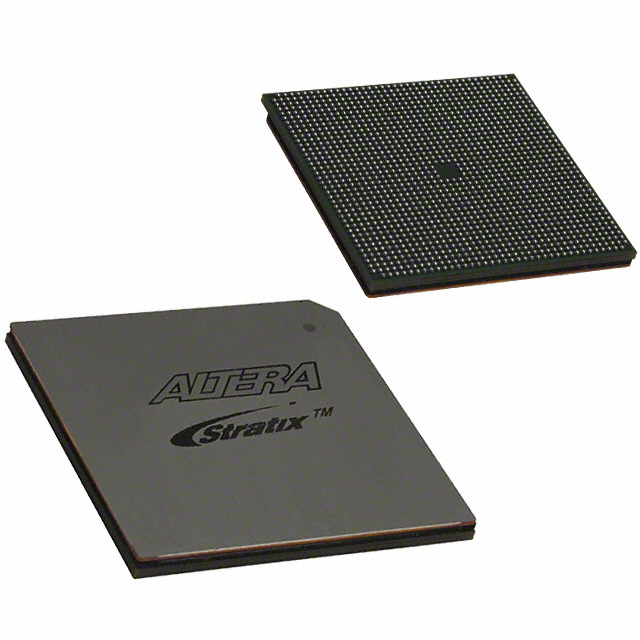
EP1S80F1508C7N
| Part Description |
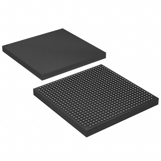
Stratix® Field Programmable Gate Array (FPGA) IC 1203 7427520 79040 1508-BBGA, FCBGA |
|---|---|
| Quantity | 278 Available (as of June 14, 2026) |

| Product Category | Field Programmable Gate Array (FPGA) |
|---|---|
| Manufacturer | Intel |
| Manufacturing Status | Obsolete |
| Manufacturer Standard Lead Time | Contact Us |
| Datasheet |
Specifications & Environmental
| Device Package | 1508-FBGA, FC (40x40) | Grade | Commercial | Operating Temperature | 0°C – 85°C | ||
|---|---|---|---|---|---|---|---|
| Package / Case | 1508-BBGA, FCBGA | Number of I/O | 1203 | Voltage | 1.425 V - 1.575 V | ||
| Mounting Method | Surface Mount | RoHS Compliance | Unknown | REACH Compliance | REACH Unaffected | ||
| Moisture Sensitivity Level | 3 (168 Hours) | Number of LABs/CLBs | 7904 | Number of Logic Elements/Cells | 79040 | ||
| Number of Gates | N/A | ECCN | 3A001A7A | HTS Code | 8542.39.0001 | ||
| Qualification | N/A | Total RAM Bits | 7427520 |
Overview of EP1S80F1508C7N – Stratix® Field Programmable Gate Array (FPGA) IC
The EP1S80F1508C7N is a Stratix® family FPGA from Intel, delivered in a 1508-ball FCBGA package for surface-mount assembly. It provides a high-density programmable fabric with a large number of logic elements and embedded memory suitable for complex digital designs.
Built for applications that require dense logic, abundant on-chip RAM and high I/O count, this commercial-grade device offers integrated clocking, DSP and I/O features documented in the Stratix device handbook and product datasheet. Key electrical and environmental parameters include a core voltage range of 1.425 V to 1.575 V and an operating temperature range of 0 °C to 85 °C.
Key Features
- Logic Capacity Approximately 79,040 logic elements, enabling implementation of large-scale digital logic and control functions.
- Embedded Memory Approximately 7.43 Mbits of on-chip RAM for buffering, tables and local storage within the FPGA fabric.
- High I/O Count 1,203 user I/O pins to support wide parallel buses, large-channel systems and complex peripheral interfacing.
- Clocking & PLLs Comprehensive clocking architecture with PLL and hierarchical clock network support as described in the Stratix device handbook for flexible timing and frequency management.
- DSP & Multiplier Resources Dedicated DSP/multiplier blocks and arithmetic support for high-throughput signal processing and computational tasks (documented in device handbook).
- I/O Structure & High-Speed Support Advanced I/O capabilities including double-data-rate and high-speed differential I/O support referenced in the device documentation for high-bandwidth interfaces.
- Configuration & Test On-chip support for JTAG boundary-scan and embedded logic analysis (SignalTap II) to simplify configuration, debugging and in-system validation.
- Package & Mounting 1508-BBGA (FCBGA) package optimized for surface-mount assembly in component-dense designs.
- Electrical & Environmental Core supply range 1.425 V–1.575 V; commercial operating temperature 0 °C–85 °C; RoHS compliant.
Typical Applications
- High-density digital systems Implement complex control logic, custom processors and state machines using the device’s large logic element count and embedded memory.
- Data buffering and packet processing Leverage approximately 7.43 Mbits of on-chip RAM and dedicated DSP resources for real-time buffering and packet handling.
- High-channel I/O systems Use 1,203 I/Os to interface with multi-lane parallel buses, sensor arrays, or large peripheral sets.
- Prototype and platform development Flexible Stratix architecture and on-chip debug/configuration features support evaluation and rapid design iteration.
Unique Advantages
- Highly scalable logic resource: Around 79k logic elements provide the headroom needed for large, complex designs without external logic expansion.
- Substantial on-chip memory: Approximately 7.43 Mbits of embedded RAM reduces dependence on external memory for many buffering and storage tasks.
- Extensive I/O capability: 1,203 I/Os support wide interfaces and high channel counts, simplifying board-level connectivity.
- Integrated timing resources: PLLs and hierarchical clock networks documented for precise clock management across the design.
- Design visibility and testability: JTAG boundary-scan and embedded SignalTap II support enable in-system test, debug and verification workflows.
- Commercial-grade, RoHS-compliant: Commercial operating range (0 °C–85 °C) and RoHS compliance support mainstream electronics manufacturing and regulatory requirements.
Why Choose EP1S80F1508C7N?
The EP1S80F1508C7N positions itself as a high-density Stratix FPGA option when your design requires a large pool of logic elements, substantial embedded RAM and a very high I/O count in a compact FCBGA package. Its documented clocking, DSP resources and on-chip debug/configuration features make it suitable for projects that demand integrated timing control, signal processing blocks and in-system visibility.
Engineers and teams targeting complex digital systems, multi-channel interfaces or platform development will find the device’s capacity and documented architecture helpful for scaling designs. Detailed device information and implementation guidance are available in the Stratix device handbook and product datasheet to support development and deployment.
Request a quote or submit a quotation request to begin procurement or to receive pricing and availability for EP1S80F1508C7N.


Date Founded: 1968
Headquarters: Santa Clara, California, USA
Employees: 130,000+
Revenue: $54.23 Billion
Certifications and Memberships: ISO9001:2015, ISO14001:2015, ISO17025:2017, ISO27001:2022, ISO45001:2018, ISO50001:2018


