
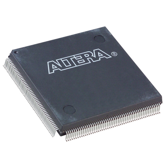
EP20K100EFI144-3
| Part Description |
APEX-20K® Field Programmable Gate Array (FPGA) IC 93 53248 4160 144-LQFP |
|---|---|
| Quantity | 341 Available (as of June 15, 2026) |

| Product Category | Field Programmable Gate Array (FPGA) |
|---|---|
| Manufacturer | Intel |
| Manufacturing Status | Obsolete |
| Manufacturer Standard Lead Time | Contact Us |
| Datasheet |
Specifications & Environmental
| Device Package | 144-TQFP (20x20) | Grade | Industrial | Operating Temperature | -40°C – 100°C | ||
|---|---|---|---|---|---|---|---|
| Package / Case | 144-LQFP | Number of I/O | 93 | Voltage | 1.71 V - 1.89 V | ||
| Mounting Method | Surface Mount | RoHS Compliance | Unknown | REACH Compliance | REACH Unknown | ||
| Moisture Sensitivity Level | 3 (168 Hours) | Number of LABs/CLBs | 416 | Number of Logic Elements/Cells | 4160 | ||
| Number of Gates | 263000 | ECCN | OBSOLETE | HTS Code | 0000.00.0000 | ||
| Qualification | N/A | Total RAM Bits | 53248 |
Overview of EP20K100EFI144-3 – APEX-20K® Field Programmable Gate Array (FPGA) IC, 144-LQFP
The EP20K100EFI144-3 is an Altera APEX-20K series FPGA provided in a 144-LQFP surface-mount package. It integrates a MultiCore architecture combining lookup-table (LUT) logic, product-term logic and embedded memory to support system-level integration and on-chip buffering.
With 4,160 logic elements, approximately 53 kbits of embedded RAM, flexible clocking and rich I/O, this industrial-grade device targets designs that require mid-range logic density, embedded memory and multi-voltage I/O compatibility within a compact 144-pin footprint.
Key Features
- Core Architecture MultiCore architecture combining LUT logic and product-term logic for register- and combinatorial-intensive functions; series-level SOPC integration capabilities.
- Logic Density 4,160 logic elements (LEs) delivering approximately 263,000 system gates to implement medium-complexity custom logic.
- Embedded Memory Approximately 53,248 bits of on-chip RAM organized as embedded system blocks suitable for FIFOs, dual-port RAM and CAM-style functions.
- I/O and Interface 93 user I/O pins with series-level support for MultiVolt I/O standards and advanced I/O protocols; designed for high-speed external memory and bus interfacing.
- Clocking and Timing Flexible clock management with up to four PLLs, built-in low-skew clock tree and programmable clock phase/delay features to support synchronous system designs.
- Power and Supply Internal and I/O supply requirements per device: specified voltage supply range of 1.71 V to 1.89 V for this part number, and series-level low-power design options.
- Package and Temperature Surface-mount 144-LQFP package (144-TQFP 20×20 supplier package) rated for industrial temperature operation from −40 °C to 100 °C.
- Design-for-Test Series documentation notes JTAG boundary-scan support for system-level testability and debug.
Typical Applications
- Embedded system integration On-chip memory and LUT resources make the device suitable for combining control logic and buffer/FIFO functions in compact system designs.
- High-speed I/O and memory interfaces Use in applications that interface to external memories and high-speed buses where flexible I/O and clocking support are required.
- Industrial control and automation Industrial-grade temperature range and surface-mount packaging fit control, monitoring and sensor aggregation tasks in industrial equipment.
- Custom logic and protocol bridging Mid-range logic density and numerous I/O pins allow implementation of protocol converters, bus bridges and glue-logic functions.
Unique Advantages
- Balanced logic and memory mix: 4,160 logic elements combined with approximately 53 kbits of embedded RAM support both logic-intensive and buffer-centric functions on a single device.
- Flexible clocking: Multiple PLLs and a low-skew clock tree provide the timing control needed for multi-domain designs and high-speed interfaces.
- Compact industrial package: 144-LQFP surface-mount package and −40 °C to 100 °C rating enable deployment in space-constrained, industrial environments.
- Rich I/O capability: 93 user I/O pins and family-level MultiVolt support facilitate interfacing to a wide range of external devices and memory technologies.
- On-board system integration: Embedded system blocks (ESBs) support FIFO, dual-port RAM and CAM implementations to reduce external component count.
Why Choose EP20K100EFI144-3?
The EP20K100EFI144-3 positions itself as a mid-density FPGA option for designers who need a compact, industrial-grade programmable device with a practical balance of logic elements and embedded memory. Its combination of 4,160 logic elements, approximately 53 kbits of embedded RAM, flexible clocking and 93 I/O pins supports integration of custom logic, buffering and interface functions in a single 144-LQFP package.
This part is suited to engineering teams building embedded platforms, I/O-intensive controllers and industrial systems that require on-chip memory and predictable clock management, while maintaining a small footprint and industrial temperature capabilities.
Request a quote or submit a pricing inquiry to receive availability and lead-time information for EP20K100EFI144-3. Provide your required quantities and delivery needs to get a prompt response.


Date Founded: 1968
Headquarters: Santa Clara, California, USA
Employees: 130,000+
Revenue: $54.23 Billion
Certifications and Memberships: ISO9001:2015, ISO14001:2015, ISO17025:2017, ISO27001:2022, ISO45001:2018, ISO50001:2018


