
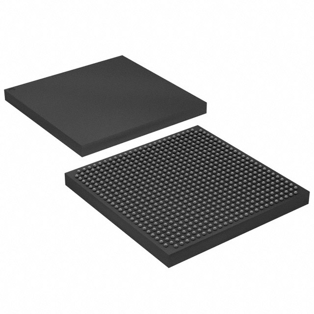
EP20K300EFC672-1
| Part Description |
APEX-20KE® Field Programmable Gate Array (FPGA) IC 408 147456 11520 672-BBGA |
|---|---|
| Quantity | 513 Available (as of October 7, 2026) |

| Product Category | Field Programmable Gate Array (FPGA) |
|---|---|
| Manufacturer | Intel |
| Manufacturing Status | Obsolete |
| Manufacturer Standard Lead Time | Contact Us |
| Datasheet |
Specifications & Environmental
| Device Package | 672-FBGA (27x27) | Grade | Commercial | Operating Temperature | 0°C – 85°C | ||
|---|---|---|---|---|---|---|---|
| Package / Case | 672-BBGA | Number of I/O | 408 | Voltage | 1.71 V - 1.89 V | ||
| Mounting Method | Surface Mount | RoHS Compliance | Unknown | REACH Compliance | REACH Unaffected | ||
| Moisture Sensitivity Level | 3 (168 Hours) | Number of LABs/CLBs | 1152 | Number of Logic Elements/Cells | 11520 | ||
| Number of Gates | 728000 | ECCN | 3A001A2A | HTS Code | 8542.39.0001 | ||
| Qualification | N/A | Total RAM Bits | 147456 |
Overview of EP20K300EFC672-1 – APEX-20KE FPGA, 672‑BBGA
The EP20K300EFC672-1 is an APEX‑20KE family field programmable gate array optimized for mid‑to‑high density system integration. It combines a MultiCore architecture with lookup‑table logic, product‑term logic and embedded memory to implement register‑intensive, combinatorial and memory functions on a single device.
Targeted for commercial applications, this surface‑mount FPGA delivers 11,520 logic elements, wide I/O flexibility and on‑chip memory resources to support complex logic, interfacing and embedded buffering within a compact 672‑ball FBGA footprint.
Key Features
- Core Architecture MultiCore architecture integrating LUT logic and product‑term logic for a mix of register‑intensive and combinatorial functions; device family documentation highlights fast, hierarchical interconnect structures and a dedicated carry chain.
- Logic Capacity Approximately 11,520 logic elements (LEs) and a maximum of 728,000 system gates provide mid‑to‑high density programmable logic resources.
- Embedded Memory Approximately 0.147 Mbits of on‑chip RAM (147,456 total RAM bits) for FIFOs, dual‑port RAM and other embedded memory functions.
- I/O and Interface Flexibility 408 user I/O pins with MultiVolt I/O support for 1.8 V, 2.5 V, 3.3 V and 5.0 V signaling. I/O features include programmable output slew‑rate control, individual tri‑state enables, pull‑ups during configuration and support for advanced standards documented for the APEX‑20K family.
- Clock Management Flexible clocking with up to four PLLs, a built‑in low‑skew clock tree and support for up to eight global clock signals. Family features include ClockLock, ClockBoost and ClockShift functions for programmable phase, delay and clock multiplication/division.
- Performance and Connectivity Family datasheet cites bidirectional I/O performance up to 250 MHz and LVDS capabilities; device-level attributes support high‑speed memory interfaces and PCI 3.3‑V operation as described for the APEX‑20K devices.
- Power and Supply Designed for low‑power operation with an internal supply range specified at 1.71 V to 1.89 V and MultiVolt I/O interface support to match a variety of peripheral devices.
- Package and Temperature Surface‑mount 672‑BBGA / 672‑FBGA (27×27) package; commercial grade with an operating temperature range of 0 °C to 85 °C.
- Standards and Reliability Family datasheet documents embedded JTAG boundary‑scan support and device features intended for robust system integration and testability.
Typical Applications
- Embedded System Integration — Use built‑in memory and mixed logic resources to implement FIFOs, dual‑port RAM and system glue logic within a single FPGA.
- High‑speed I/O and Interfaces — Leverage MultiVolt I/O and documented PCI 3.3‑V support for bridging and peripheral interfacing.
- Memory Subsystem Support — Support high‑speed external memory interfaces and on‑chip buffering for SDRAM and SRAM applications.
- Clock‑centric Designs — Take advantage of multiple PLLs and clock management features for designs requiring phase control, clock multiplication or low skew distribution.
Unique Advantages
- Compact, mid‑range density: 11,520 logic elements and 147,456 RAM bits provide a balance of logic and embedded memory for consolidated designs without large device overhead.
- Flexible I/O voltage support: MultiVolt I/O compatibility enables direct interfacing to a wide range of peripherals and I/O standards.
- Advanced clocking options: Up to four PLLs and family clock features simplify timing architectures for multi‑clock systems.
- System testability: Embedded JTAG boundary‑scan capabilities facilitate board‑level bring‑up and in‑system testing.
- Commercial temperature rating: Specified 0 °C to 85 °C operation for standard commercial applications and environments.
- Space‑efficient package: 672‑ball FBGA (27×27) offers a high‑pin‑count solution in a compact surface‑mount footprint.
Why Choose EP20K300EFC672-1?
The EP20K300EFC672-1 provides a balanced combination of logic capacity, embedded memory and flexible I/O in a compact 672‑ball FBGA package. Its MultiCore architecture and on‑chip resources make it well suited for designs that require integrated FIFOs, interface bridging, and multi‑clock management while maintaining a commercially rated temperature range.
This device is appropriate for engineering teams building mid‑density, performance‑focused systems that benefit from on‑chip memory, programmable clocking and broad I/O voltage support. The APEX‑20K family documentation and device features support straightforward integration into systems where testability, configurable logic and interface flexibility are priorities.
Request a quote or submit an RFQ to receive pricing and availability information for the EP20K300EFC672-1. Provide your component quantity and required lead time to initiate the quote process.

























Date Founded: 1968
Headquarters: Santa Clara, California, USA
Employees: 130,000+
Revenue: $54.23 Billion
Certifications and Memberships: ISO9001:2015, ISO14001:2015, ISO17025:2017, ISO27001:2022, ISO45001:2018, ISO50001:2018


