
EP20K300EFC672-2
| Part Description |
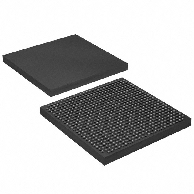
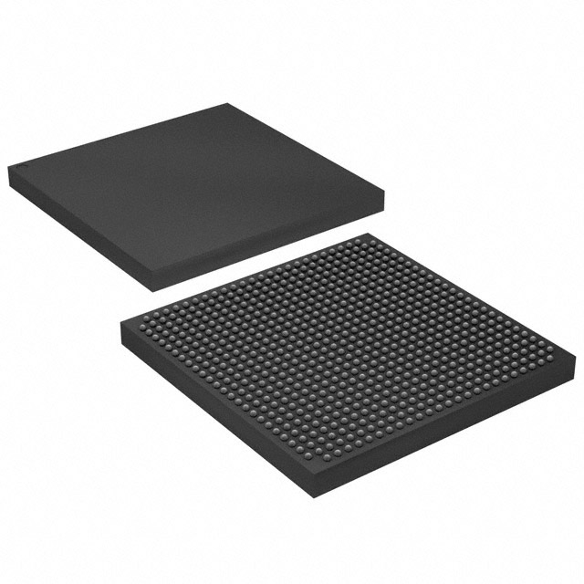
APEX-20KE® Field Programmable Gate Array (FPGA) IC 408 147456 11520 672-BBGA |
|---|---|
| Quantity | 162 Available (as of October 8, 2026) |
| Product Category | Field Programmable Gate Array (FPGA) |
|---|---|
| Manufacturer | Intel |
| Manufacturing Status | Obsolete |
| Manufacturer Standard Lead Time | Contact Us |
| Datasheet |
Specifications & Environmental
| Device Package | 672-FBGA (27x27) | Grade | Commercial | Operating Temperature | 0°C – 85°C | ||
|---|---|---|---|---|---|---|---|
| Package / Case | 672-BBGA | Number of I/O | 408 | Voltage | 1.71 V - 1.89 V | ||
| Mounting Method | Surface Mount | RoHS Compliance | RoHS non-compliant | REACH Compliance | REACH Unaffected | ||
| Moisture Sensitivity Level | 3 (168 Hours) | Number of LABs/CLBs | 1152 | Number of Logic Elements/Cells | 11520 | ||
| Number of Gates | 728000 | ECCN | 3A991D | HTS Code | 8542.39.0001 | ||
| Qualification | N/A | Total RAM Bits | 147456 |
Overview of EP20K300EFC672-2 – APEX-20KE® Field Programmable Gate Array (FPGA) IC 408 147456 11520 672-BBGA
The EP20K300EFC672-2 is a high-density APEX-20KE® FPGA optimized for system-on-a-programmable-chip integration. It combines a MultiCore architecture with look-up table (LUT) logic, product-term logic and embedded memory to support complex, tightly integrated digital designs.
Designed for commercial applications, this device delivers substantial logic and I/O resources—including 11,520 logic elements, approximately 0.147 Mbits of embedded memory and 408 I/O pins—while operating from a 1.71 V to 1.89 V supply and a 0 °C to 85 °C temperature range.
Key Features
- Core architecture MultiCore architecture integrating LUT logic and product-term logic for flexible implementation of both register‑intensive and combinatorial functions.
- Logic capacity 11,520 logic elements and up to 728,000 system gates provide substantial on‑chip logic resources for high-density designs.
- Embedded memory Approximately 0.147 Mbits of on‑chip RAM, with embedded system blocks (ESBs) that can implement FIFOs, dual‑port RAM and CAM functions.
- I/O and interfacing 408 I/O pins with MultiVolt I/O support for interfacing across common voltage domains and programmable output slew and clamp features for signal integrity control.
- Clock management Built‑in clock resources including multiple PLLs, a low‑skew clock tree and features for phase/delay adjustment to simplify timing distribution.
- Package and mounting 672‑ball BGA package (supplier device package: 672‑FBGA, 27×27) in a surface‑mount form factor for compact board integration.
- Power and temperature Internal operating supply between 1.71 V and 1.89 V and commercial operating temperature range of 0 °C to 85 °C.
- Standards and performance features Family-level features include high‑speed I/O options (including LVDS capability) and support for common memory interfaces and PCI signaling as implemented across the APEX‑20K family.
- RoHS compliance Device is RoHS compliant for environmental conformity.
Typical Applications
- Memory‑intensive buffering and FIFO logic Use embedded system blocks to implement FIFO buffers, dual‑port RAM and CAMs for data buffering and packet staging.
- Custom I/O and protocol bridging Implement multi‑voltage I/O interfaces and high‑speed signaling to bridge between different system domains or legacy interfaces.
- System integration and SOPC designs Integrate control logic, peripherals and on‑chip memory for compact system‑on‑a‑programmable‑chip solutions.
- High‑density logic implementations Deploy large combinatorial and register‑rich logic blocks enabled by 11,520 logic elements and extensive interconnect resources.
Unique Advantages
- High logic density: 11,520 logic elements and up to 728,000 system gates enable large, complex designs on a single device.
- Embedded memory flexibility: Approximately 0.147 Mbits of on‑chip RAM and ESB features for FIFOs and dual‑port RAM reduce external memory dependencies.
- Rich I/O resource set: 408 I/O pins with MultiVolt support provide flexible interfacing across multiple voltage domains and signal standards.
- Robust clocking options: Multiple PLLs and a low‑skew clock tree simplify clock distribution and timing control for synchronous systems.
- Compact, surface‑mount package: 672‑ball BGA (27×27) balances high pin count with a compact PCB footprint for space‑constrained designs.
- Commercial temperature and RoHS compliance: Rated for 0 °C to 85 °C operation and RoHS compliant for standard commercial applications.
Why Choose EP20K300EFC672-2?
The EP20K300EFC672-2 positions itself as a scalable, integration‑focused FPGA for commercial designs that require high logic density, flexible embedded memory and broad I/O capabilities. Its MultiCore architecture and ESB features let engineers consolidate logic and memory functions on‑chip, reducing system complexity and BOM count.
This device is suited for customers implementing complex digital systems, memory controllers, protocol bridges and SOPC architectures who need a combination of logic capacity, embedded RAM and extensive I/O in a compact BGA package with commercial temperature support.
Request a quote or submit a pricing inquiry to learn more about availability, lead times and volume options for the EP20K300EFC672-2.
























Date Founded: 1968
Headquarters: Santa Clara, California, USA
Employees: 130,000+
Revenue: $54.23 Billion
Certifications and Memberships: ISO9001:2015, ISO14001:2015, ISO17025:2017, ISO27001:2022, ISO45001:2018, ISO50001:2018


