
EP20K300EFC672-2N
| Part Description |
APEX-20KE® Field Programmable Gate Array (FPGA) IC 408 147456 11520 672-BBGA |
|---|---|
| Quantity | 1,213 Available (as of June 14, 2026) |
| Product Category | Field Programmable Gate Array (FPGA) |
|---|---|
| Manufacturer | Intel |
| Manufacturing Status | Obsolete |
| Manufacturer Standard Lead Time | Contact Us |
| Datasheet |
Specifications & Environmental
| Device Package | 672-FBGA (27x27) | Grade | Commercial | Operating Temperature | 0°C – 85°C | ||
|---|---|---|---|---|---|---|---|
| Package / Case | 672-BBGA | Number of I/O | 408 | Voltage | 1.71 V - 1.89 V | ||
| Mounting Method | Surface Mount | RoHS Compliance | Unknown | REACH Compliance | REACH Unaffected | ||
| Moisture Sensitivity Level | 3 (168 Hours) | Number of LABs/CLBs | 1152 | Number of Logic Elements/Cells | 11520 | ||
| Number of Gates | 728000 | ECCN | 3A991D | HTS Code | 8542.39.0001 | ||
| Qualification | N/A | Total RAM Bits | 147456 |
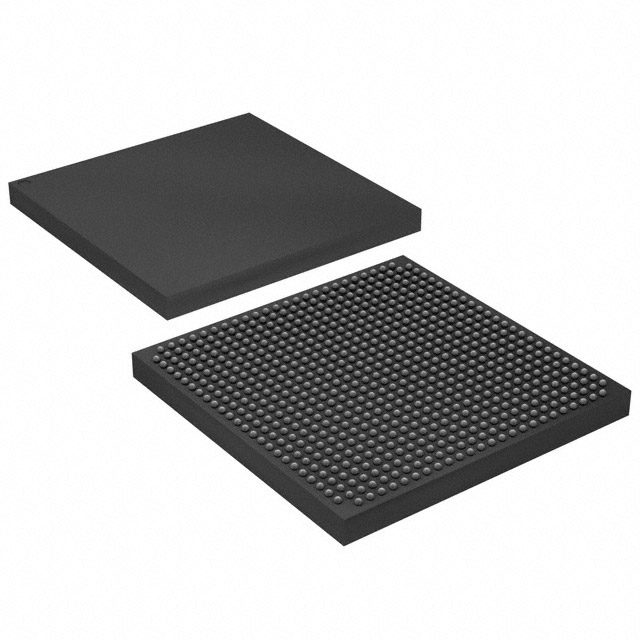
Overview of EP20K300EFC672-2N – APEX-20KE® FPGA, 11,520 logic elements, 147,456-bit RAM, 408 I/Os, 672-BBGA
The EP20K300EFC672-2N is an Intel APEX-20KE® field programmable gate array (FPGA) in a 672-BBGA package, offering a high-density programmable logic platform for commercial designs. It implements the APEX 20K family MultiCore architecture with LUT logic, product-term logic and embedded system blocks for on-chip memory and combinatorial functions.
With 11,520 logic elements, approximately 147,456 bits of embedded memory, and 408 user I/Os, this device targets applications that require significant on-chip logic and memory capacity with flexible I/O and clock management in a surface-mount, commercial-grade package.
Key Features
- Logic Capacity — 11,520 logic elements and up to 728,000 system gates (family listing) provide substantial programmable logic for complex designs.
- On-chip Memory — Approximately 0.147 Mbits of embedded memory (147,456 bits) implemented in Embedded System Blocks (ESBs) for FIFOs, dual-port RAM and CAM-style functions.
- I/O Density & Flexibility — 408 user I/Os with MultiVolt I/O interface support across the APEX 20K family for interfacing with multiple voltage domains; programmable output slew-rate and individual tri-state control.
- Clock Management — Family features include up to four PLLs, a built-in low-skew clock tree and up to eight global clock signals, along with ClockLock, ClockBoost and ClockShift capabilities for phase and delay control.
- High-speed Interfaces — APEX 20K family supports high-speed I/O standards and memory interfaces including DDR SDRAM and LVDS performance (family-level specifications).
- Power & Supply — Internal supply and device operation designed for low-power operation; device voltage supply is specified at 1.71 V to 1.89 V for this part.
- Package & Mounting — 672-BBGA package; supplier device package listed as 672-FBGA (27×27) and surface-mount mounting for compact board-level integration.
- Commercial Temperature Grade — Rated for 0 °C to 85 °C operating temperature; intended for commercial applications. RoHS compliant.
Typical Applications
- Memory Interface & Controllers — Implement DDR SDRAM controllers, FIFOs and high-bandwidth buffering using ESBs and on-chip memory resources.
- High-speed I/O Systems — Systems requiring many I/Os and support for LVDS and other high-speed standards can leverage the device's flexible I/O and clocking features.
- PCI and Bus-Based Designs — APEX 20K family support for PCI signaling (family-level) suits embedded PCI Local Bus applications at 3.3-V operation.
- Complex Logic Integration — Consolidate multiple logic functions and glue logic into a single FPGA to reduce BOM and simplify board design.
Unique Advantages
- Highly integrated MultiCore architecture: Combines LUT logic, product-term logic and ESBs to implement both logic and on-chip memory functions within the same device.
- Substantial on-chip resources: 11,520 logic elements and 147,456 bits of embedded RAM enable mid-to-high density designs without external memory for many functions.
- Flexible clocking: Multiple PLLs, global clocks and programmable clock features allow precise timing control for synchronous systems.
- Versatile I/O capability: 408 I/Os and family-level MultiVolt and high-speed interface support simplify system-level interfacing across voltage domains.
- Compact surface-mount package: 672-BBGA (supplier 672-FBGA, 27×27) provides high pin-count in a compact footprint for space-constrained PCBs.
- Commercial-grade qualification: Operates across a 0 °C to 85 °C range and is RoHS compliant for standard commercial deployments.
Why Choose EP20K300EFC672-2N?
The EP20K300EFC672-2N positions itself for designers who need a commercially qualified, high-density FPGA with substantial on-chip memory and extensive I/O. Its APEX MultiCore architecture and embedded system blocks enable integration of complex logic and memory functions, while family-level clocking and I/O features provide design flexibility for high-performance data paths and memory interfaces.
Choose this device when you require a compact, surface-mount FPGA that balances logic capacity, embedded memory, and I/O density for commercial embedded systems, communications, and interface-intensive applications. Its combination of programmable resources and family-level features supports scalable designs and reduces external component count.
Request a quote or contact sales to discuss availability, pricing and how EP20K300EFC672-2N can fit your next design.


Date Founded: 1968
Headquarters: Santa Clara, California, USA
Employees: 130,000+
Revenue: $54.23 Billion
Certifications and Memberships: ISO9001:2015, ISO14001:2015, ISO17025:2017, ISO27001:2022, ISO45001:2018, ISO50001:2018


