
EP20K300EFC672-1X
| Part Description |
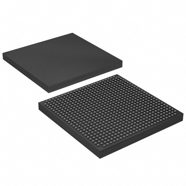
APEX-20KE® Field Programmable Gate Array (FPGA) IC 408 147456 11520 672-BBGA |
|---|---|
| Quantity | 116 Available (as of June 14, 2026) |

| Product Category | Field Programmable Gate Array (FPGA) |
|---|---|
| Manufacturer | Intel |
| Manufacturing Status | Obsolete |
| Manufacturer Standard Lead Time | Contact Us |
| Datasheet |
Specifications & Environmental
| Device Package | 672-FBGA (27x27) | Grade | Commercial | Operating Temperature | 0°C – 85°C | ||
|---|---|---|---|---|---|---|---|
| Package / Case | 672-BBGA | Number of I/O | 408 | Voltage | 1.71 V - 1.89 V | ||
| Mounting Method | Surface Mount | RoHS Compliance | Unknown | REACH Compliance | REACH Unaffected | ||
| Moisture Sensitivity Level | 3 (168 Hours) | Number of LABs/CLBs | 1152 | Number of Logic Elements/Cells | 11520 | ||
| Number of Gates | 728000 | ECCN | 3A001A2A | HTS Code | 8542.39.0001 | ||
| Qualification | N/A | Total RAM Bits | 147456 |
Overview of EP20K300EFC672-1X – APEX-20KE Field Programmable Gate Array (FPGA), 672-BBGA
The EP20K300EFC672-1X is an APEX-20KE family FPGA delivering high-density programmable logic in a 672-BBGA package. Built around a MultiCore architecture with LUT logic and embedded system blocks (ESBs), this commercial-grade device targets applications requiring substantial on-chip logic, embedded memory and flexible I/O connectivity.
With 11,520 logic elements, approximately 0.147 Mbits of embedded memory and 408 I/O pins, the EP20K300EFC672-1X is suited to board-level systems that need integrated memory functions, configurable clock management and multi-voltage I/O support.
Key Features
- Core Architecture MultiCore architecture combining look-up table (LUT) logic and product-term logic for register- and combinatorial-intensive functions.
- Logic Density 11,520 logic elements and a maximum of 728,000 system gates enable substantial programmable logic capacity for medium-to-high complexity designs.
- Embedded Memory Approximately 0.147 Mbits of on-chip RAM provided by embedded system blocks (ESBs) for FIFO buffers, dual-port RAM and CAM implementations.
- I/O Capacity & Flexibility 408 user I/O pins with MultiVolt I/O interface support, programmable output slew-rate control, individual tri-state enable control and programmable clamp to VCCIO.
- Clock Management Flexible clock circuitry with up to four PLLs, a built-in low-skew clock tree and features such as ClockLock, ClockBoost and ClockShift for phase and delay control.
- Memory & Bus Support Architecture supports high-speed external memory interfaces (including DDR SDRAM and ZBT SRAM) and is compatible with PCI Local Bus operation at 3.3 V as specified in the device family documentation.
- Performance I/O Standards Support for high-speed standards including LVDS (up to 840 Mbits/channel reported in the family datasheet) and other advanced I/O signaling options.
- Package & Mounting Surface-mount 672-BBGA package (supplier device package listed as 672-FBGA (27x27)).
- Power & Operating Range Device internal supply as provided: voltage supply 1.71 V to 1.89 V; commercial operating temperature range 0 °C to 85 °C.
- Compliance RoHS compliant.
Typical Applications
- High-speed memory interfaces — Embedded memory and ESB features support implementation of FIFO buffers and dual-port RAM for DDR and ZBT memory controllers.
- PCI-based systems — Family-level PCI Local Bus compliance for 3.3 V operation enables implementation of PCI/legacy bus logic and bridging functions.
- High-performance I/O and serial links — LVDS and multi-standard I/O support facilitate high-bandwidth channel interfaces and custom protocol implementation.
- Custom embedded logic — 11,520 logic elements and extensive I/O make this device suitable for control, signal processing glue logic, and mid-density FPGA tasks on commercial boards.
Unique Advantages
- Substantial on-chip logic: 11,520 logic elements deliver programmable capacity for complex glue logic, state machines and processing pipelines without immediate external ASIC development.
- Integrated embedded memory: ESBs providing approximately 0.147 Mbits of RAM simplify implementation of FIFOs, buffers and small data stores, reducing external memory dependence.
- Robust I/O versatility: 408 user I/Os with MultiVolt support and advanced I/O controls enable flexible interfacing across multiple voltage domains and signaling standards.
- Configurable clocking: Multiple PLLs and clock-control features help implement low-skew multi-clock designs and frequency/phase adjustments on-chip.
- Commercial temperature rating: Specified 0 °C to 85 °C operating range aligns with standard commercial product deployments.
- RoHS compliant: Meets lead-free and material compliance expectations for commercial electronics production.
Why Choose EP20K300EFC672-1X?
The EP20K300EFC672-1X positions itself as a mid-to-high density FPGA option within the APEX-20KE family, combining a MultiCore LUT-based architecture, embedded memory blocks and broad I/O capability in a compact 672-BBGA form factor. Its balance of logic elements, on-chip RAM and 408 I/Os makes it appropriate for designers building commercial board-level systems that require integrated memory functions, flexible clocking and multi-standard I/O support.
For teams and projects that need an FPGA with verifiable family-level features—such as PLL-based clock management, support for high-speed memory interfaces and LVDS channels—this device delivers those capabilities while maintaining commercial-grade operating parameters and RoHS compliance.
Request a quote or submit a procurement inquiry to receive pricing, availability and additional technical support for the EP20K300EFC672-1X.


Date Founded: 1968
Headquarters: Santa Clara, California, USA
Employees: 130,000+
Revenue: $54.23 Billion
Certifications and Memberships: ISO9001:2015, ISO14001:2015, ISO17025:2017, ISO27001:2022, ISO45001:2018, ISO50001:2018


