
EP20K30ETC144-3N
| Part Description |
APEX-20KE® Field Programmable Gate Array (FPGA) IC 92 24576 1200 144-LQFP |
|---|---|
| Quantity | 484 Available (as of June 15, 2026) |

| Product Category | Field Programmable Gate Array (FPGA) |
|---|---|
| Manufacturer | Intel |
| Manufacturing Status | Obsolete |
| Manufacturer Standard Lead Time | Contact Us |
| Datasheet |
Specifications & Environmental
| Device Package | 144-TQFP (20x20) | Grade | Commercial | Operating Temperature | 0°C – 85°C | ||
|---|---|---|---|---|---|---|---|
| Package / Case | 144-LQFP | Number of I/O | 92 | Voltage | 1.71 V - 1.89 V | ||
| Mounting Method | Surface Mount | RoHS Compliance | Unknown | REACH Compliance | REACH Unaffected | ||
| Moisture Sensitivity Level | 3 (168 Hours) | Number of LABs/CLBs | 120 | Number of Logic Elements/Cells | 1200 | ||
| Number of Gates | 113000 | ECCN | 3A991D | HTS Code | 8542.39.0001 | ||
| Qualification | N/A | Total RAM Bits | 24576 |
Overview of EP20K30ETC144-3N – APEX-20KE® FPGA, 1,200 Logic Elements, 24,576 bits RAM, 144-LQFP
The EP20K30ETC144-3N is an APEX-20KE® field programmable gate array (FPGA) in a 144-LQFP package designed for commercial applications. It implements a MultiCore architecture that integrates look-up table (LUT) logic, product-term logic, and embedded memory to enable system-on-a-programmable-chip integration for control, interface, and memory-centric designs.
With 1,200 logic elements, 24,576 bits of on-chip RAM, up to 92 I/O pins and a compact 144-pin surface-mount package, this device targets I/O-rich embedded systems, memory-interface blocks, and custom logic functions where moderate density and flexible I/O are required.
Key Features
- Core Architecture MultiCore architecture integrating LUT logic and product-term logic for register- and combinatorial-intensive functions; family-level support for embedded system blocks (ESBs).
- Logic Density Approximately 1,200 logic elements and up to 113,000 system gates as specified for the device family.
- Embedded Memory 24,576 bits of on-chip RAM with ESB support for FIFO, dual-port RAM, and CAM implementations (family-level ESB capability).
- I/O and Interface Flexibility 92 user I/O pins and MultiVolt I/O interface support to interoperate with 1.8 V, 2.5 V, 3.3 V and 5.0 V signaling (family-level MultiVolt support).
- Clock Management Family-level clock resources include up to four PLLs, a built-in low-skew clock tree, up to eight global clock signals, and programmable clock features such as ClockLock, ClockBoost and ClockShift.
- High-speed I/O Options Family-level support for high-speed peripherals including LVDS channels (family LVDS performance up to 840 Mbits per channel) and support for external memory interfaces such as DDR SDRAM and ZBT SRAM.
- Power and Supply Internal supply around 1.8 V (device supply range 1.71 V to 1.89 V) with family-level options for low-power operation and programmable ESB power-saving modes.
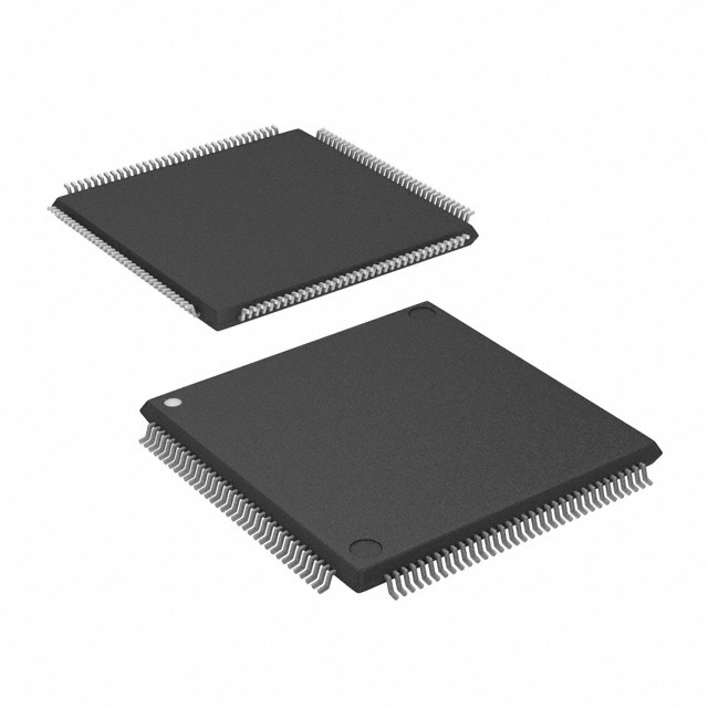
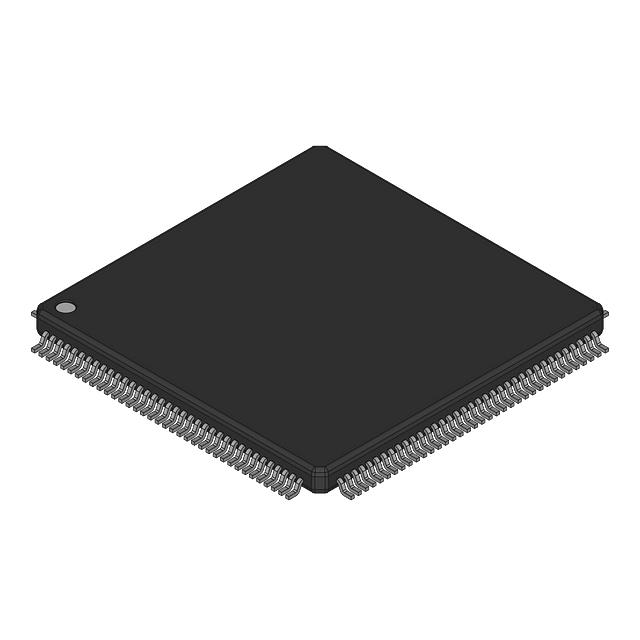
- Package & Mounting 144-LQFP surface-mount package (supplier device package: 144-TQFP, 20 × 20 mm) suitable for compact board layouts.
- Commercial Temperature Range Rated for commercial operation from 0 °C to 85 °C.
- Standards & Testability Family-level JTAG boundary-scan support is provided (boundary-scan circuitry contributes additional gates for testability).
- Regulatory RoHS compliant.
Typical Applications
- Embedded System Integration – Implement custom control logic, protocol bridging, or glue logic where integrated LUTs and ESBs simplify system design.
- Memory Interface Controllers – Use the device’s embedded memory and family-level support for DDR SDRAM and ZBT SRAM to build memory controllers and FIFO buffers.
- High-speed I/O and Interface Bridging – Leverage MultiVolt I/O and family-level LVDS capability for high-speed data channels and interface conversion.
- PCI and Bus Interfaces – Family-level compliance with PCI Local Bus Specification (3.3 V operation) enables use in PCI bus bridging and expansion applications.
Unique Advantages
- MultiCore Integration: Combines LUT logic, product-term logic, and embedded memory to reduce system component count and simplify implementation of mixed logic and memory functions.
- Balanced Logic and Memory Resources: 1,200 logic elements paired with 24,576 bits of on-chip RAM provide a compact platform for designs that require both logic and local buffering.
- Flexible I/O Support: MultiVolt I/O and a 92-pin I/O count let the device interface with a wide range of voltage domains and external devices without extensive level-shifting hardware.
- Programmable Clocking: On-chip PLLs and clock features (ClockLock, ClockBoost, ClockShift) provide designers with programmable clock multiplication, division and phase control for timing-critical designs.
- Compact Surface-Mount Package: The 144-LQFP (20 × 20 mm) package supports dense PCB layouts while offering ample I/O for moderate-complexity systems.
- Commercial-grade Reliability: Rated for 0 °C to 85 °C operation and RoHS compliant for mainstream commercial deployments.
Why Choose EP20K30ETC144-3N?
The EP20K30ETC144-3N provides a balanced FPGA option for commercial embedded designs that require moderate logic density, on-chip RAM, flexible I/O, and integrated clock management in a compact 144-pin package. Its MultiCore architecture and family-level embedded system blocks enable efficient implementation of combined logic and memory functions, reducing BOM and simplifying board-level design.
This device is well suited to customers building control logic, memory interfaces, and I/O-rich modules who need a commercially rated FPGA with programmable clocking and MultiVolt I/O support. Its combination of logic elements, embedded RAM, and I/O flexibility offers a scalable building block within the APEX 20K family.
Request a quote or submit an inquiry to receive pricing and availability for EP20K30ETC144-3N. Our team can assist with lead times and order placement.


Date Founded: 1968
Headquarters: Santa Clara, California, USA
Employees: 130,000+
Revenue: $54.23 Billion
Certifications and Memberships: ISO9001:2015, ISO14001:2015, ISO17025:2017, ISO27001:2022, ISO45001:2018, ISO50001:2018


