
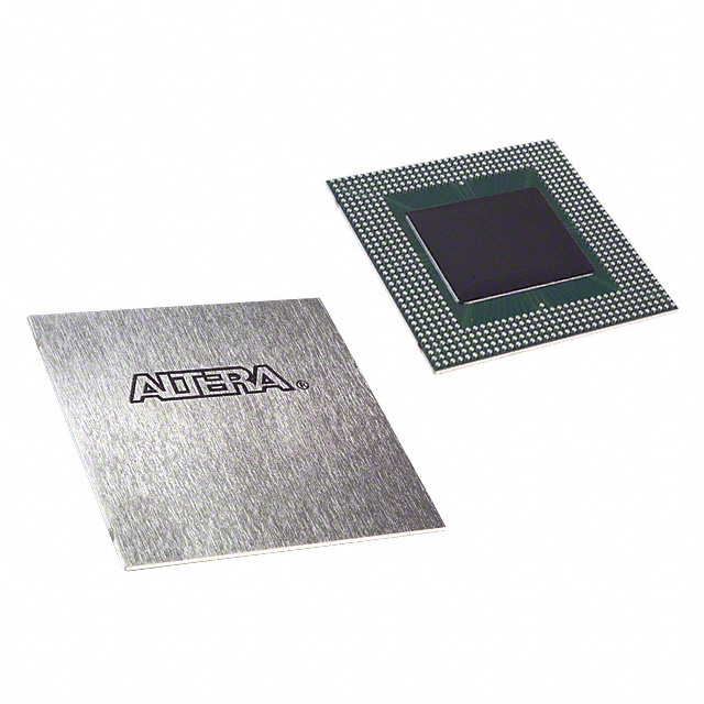
EP20K400EBC652-1X
| Part Description |
APEX-20KE® Field Programmable Gate Array (FPGA) IC 488 212992 16640 652-BGA |
|---|---|
| Quantity | 197 Available (as of June 18, 2026) |

| Product Category | Field Programmable Gate Array (FPGA) |
|---|---|
| Manufacturer | Intel |
| Manufacturing Status | Obsolete |
| Manufacturer Standard Lead Time | Contact Us |
| Datasheet |
Specifications & Environmental
| Device Package | 652-BGA (45x45) | Grade | Commercial | Operating Temperature | 0°C – 85°C | ||
|---|---|---|---|---|---|---|---|
| Package / Case | 652-BGA | Number of I/O | 488 | Voltage | 1.71 V - 1.89 V | ||
| Mounting Method | Surface Mount | RoHS Compliance | RoHS non-compliant | REACH Compliance | REACH Unaffected | ||
| Moisture Sensitivity Level | 3 (168 Hours) | Number of LABs/CLBs | 1664 | Number of Logic Elements/Cells | 16640 | ||
| Number of Gates | 1052000 | ECCN | 3A001A7A | HTS Code | 8542.39.0001 | ||
| Qualification | N/A | Total RAM Bits | 212992 |
Overview of EP20K400EBC652-1X – APEX-20KE FPGA, 652-BGA
The EP20K400EBC652-1X is an APEX-20KE® field programmable gate array (FPGA) in a 652-BGA (45×45) surface-mount package. It combines a MultiCore architecture with embedded system blocks to deliver high-density logic and on-chip memory suitable for complex programmable logic tasks.
Designed for commercial-grade applications, this device targets system integration, custom I/O interfacing, and memory-intensive logic functions where a dense, programmable solution with flexible I/O and clock management is required.
Key Features
- Core Architecture MultiCore architecture integrating look-up table (LUT) logic and product-term logic for a flexible mix of register- and combinatorial-intensive functions.
- Logic Density 16,640 logic elements supporting a total of 1,052,000 system gates to implement complex logic designs.
- Embedded Memory Approximately 0.213 Mbits of embedded memory (212,992 total RAM bits) and embedded system blocks (ESBs) for FIFO, dual-port RAM, and CAM implementations.
- I/O & Interface Flexibility 488 user I/O pins with MultiVolt I/O interface support for 1.8 V, 2.5 V, 3.3 V, and 5.0 V devices; supports high-speed external memories including DDR SDRAM and ZBT SRAM.
- Clock Management Flexible clock circuitry with up to four phase-locked loops (PLLs), up to eight global clock signals, and features such as ClockLock, ClockBoost, and ClockShift for programmable phase and delay control.
- Power and Supply Internal supply operation within the specified 1.71 V to 1.89 V range, with device-level power-saving modes available in ESBs.
- Package & Mounting 652-BGA (45×45) surface-mount package optimized for board-level integration in compact designs.
- Compliance RoHS-compliant construction suitable for commercial applications.
Typical Applications
- Networking & Communications Implement protocol engines, custom packet processing, and interface bridging using the device’s high logic density and flexible I/O.
- Memory Subsystems Design DDR SDRAM or ZBT SRAM controllers and FIFO buffers leveraging embedded system blocks and on-chip RAM.
- Embedded System Integration Consolidate glue logic, custom peripherals, and system-level glue into a single FPGA for prototype and production systems.
- High-performance I/O Implement multi-voltage interface logic and high-speed serial/parallel I/O functions across 488 user pins.
Unique Advantages
- High-density programmable logic: 16,640 logic elements and over 1,052,000 gates let you implement large, complex designs on a single device.
- On-chip memory and ESBs: Approximately 0.213 Mbits of embedded RAM plus ESBs for FIFOs, dual-port RAM, and CAM reduce external memory dependency and simplify board design.
- Flexible I/O compatibility: MultiVolt I/O support enables direct interfacing with a wide range of peripheral voltages and high-speed external memory standards.
- Advanced clock control: Up to four PLLs, multiple global clocks, and programmable clock features give precise timing control for synchronous systems.
- Compact, production-ready package: 652-BGA (45×45) surface-mount package supports dense board layouts while meeting RoHS requirements.
Why Choose EP20K400EBC652-1X?
The EP20K400EBC652-1X positions itself as a high-density, commercially graded FPGA for designs that require substantial logic capacity, embedded memory, and flexible I/O in a single, compact package. Its combination of MultiCore architecture, ESBs, and advanced clock features makes it suitable for developers consolidating multiple functions into one programmable device.
This device is appropriate for engineering teams building complex communication, memory-control, and system-integration solutions that benefit from on-chip RAM, configurable I/O voltages, and programmable clock management—backed by RoHS-compliant manufacturing and surface-mount packaging for production deployment.
If you would like pricing information or availability, request a quote or submit an inquiry to receive a sales response tailored to your volume and delivery needs.


Date Founded: 1968
Headquarters: Santa Clara, California, USA
Employees: 130,000+
Revenue: $54.23 Billion
Certifications and Memberships: ISO9001:2015, ISO14001:2015, ISO17025:2017, ISO27001:2022, ISO45001:2018, ISO50001:2018


