
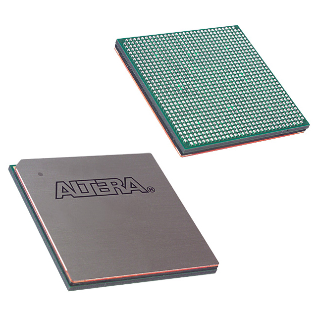
EP20K600EBC652-2X
| Part Description |
APEX-20KE® Field Programmable Gate Array (FPGA) IC 488 311296 24320 652-BGA |
|---|---|
| Quantity | 101 Available (as of June 15, 2026) |

| Product Category | Field Programmable Gate Array (FPGA) |
|---|---|
| Manufacturer | Intel |
| Manufacturing Status | Obsolete |
| Manufacturer Standard Lead Time | Contact Us |
| Datasheet |
Specifications & Environmental
| Device Package | 652-BGA (45x45) | Grade | Commercial | Operating Temperature | 0°C – 85°C | ||
|---|---|---|---|---|---|---|---|
| Package / Case | 652-BGA | Number of I/O | 488 | Voltage | 1.71 V - 1.89 V | ||
| Mounting Method | Surface Mount | RoHS Compliance | Unknown | REACH Compliance | REACH Unaffected | ||
| Moisture Sensitivity Level | 3 (168 Hours) | Number of LABs/CLBs | 2432 | Number of Logic Elements/Cells | 24320 | ||
| Number of Gates | 1537000 | ECCN | 3A001A2A | HTS Code | 8542.39.0001 | ||
| Qualification | N/A | Total RAM Bits | 311296 |
Overview of EP20K600EBC652-2X – APEX-20KE® Field Programmable Gate Array (FPGA) IC 488 311296 24320 652-BGA
The EP20K600EBC652-2X is an APEX-20KE series field programmable gate array (FPGA) in a 652-ball BGA (45×45) package. It implements the APEX 20K MultiCore architecture combining look-up table (LUT) logic, product-term logic, and embedded memory to support configurable system integration on a single device.
With 24,320 logic elements, approximately 0.31 Mbits of embedded memory, and 488 user I/O pins, this commercial-grade, surface-mount device targets designs that require high logic density, flexible I/O, and integrated clock management within a 0 °C to 85 °C operating range.
Key Features
- Core Architecture APEX 20K MultiCore architecture integrating LUT logic, product-term logic, and embedded system blocks (ESBs) for a mix of register-intensive and memory/combinatorial functions.
- Logic Density 24,320 logic elements and approximately 1.537 million system gates provide significant on-chip logic capacity for complex designs.
- Embedded Memory Approximately 0.31 Mbits of on-chip RAM (311,296 total RAM bits) for FIFOs, dual-port RAM, and CAM-style implementations using ESBs.
- I/O and Interface Flexibility 488 user I/Os with family-level MultiVolt I/O interface support (1.8 V, 2.5 V, 3.3 V, 5.0 V) and support for high-speed interfaces including LVDS and memory interfaces.
- Clock Management Flexible clock circuitry with up to four PLLs, a built-in low-skew clock tree, up to eight global clock signals, and programmable clock features such as ClockLock, ClockBoost, and ClockShift.
- Performance-Oriented I/O Features for high-speed external memory support and bidirectional I/O performance; LVDS performance up to 840 Mbits per channel (family feature).
- Package & Mounting 652-BGA (45×45) supplier device package, surface-mount construction for compact, high-density board layouts.
- Power & Operating Range Internal supply range listed at 1.71 V to 1.89 V; rated operating temperature 0 °C to 85 °C. RoHS compliant.
Typical Applications
- Memory-Intensive Designs Use the ESBs and on-chip RAM for implementing FIFOs, dual-port RAM, and memory controllers where embedded memory reduces external component count.
- High-Speed I/O Interfaces Implement LVDS lanes, high-speed peripheral interfaces, and direct memory connections leveraging the device’s high I/O count and family-level high-speed I/O support.
- Custom Logic and Integration Consolidate glue logic, protocol handling, and custom datapaths on-chip using the device’s large logic element count and rich interconnect structure.
- Clocked Systems Designs requiring multiple programmable clocks, PLL-based clock multiplication/division, or fine phase/delay control benefit from the integrated clock-management features.
Unique Advantages
- High on-chip logic capacity: 24,320 logic elements and ~1.537 million system gates allow substantial logic integration without immediate reliance on external CPLDs or ASICs.
- Embedded memory for system integration: Approximately 0.31 Mbits of RAM in ESBs supports FIFOs and dual-port RAM functions, reducing board-level memory requirements.
- Flexible clocking and timing: Up to four PLLs, an integrated low-skew clock tree, and multiple programmable clock features simplify timing architectures for complex synchronous designs.
- Broad I/O flexibility: 488 I/Os with MultiVolt family support and high-speed signaling options enable direct interfacing to a wide range of logic levels and peripherals.
- Compact, surface-mount BGA: 652-ball BGA (45×45) package supports dense PCB routing and volume manufacturing processes.
- Regulatory and manufacturing readiness: RoHS compliance and standard commercial-grade temperature range support mainstream production environments.
Why Choose EP20K600EBC652-2X?
The EP20K600EBC652-2X delivers a balanced combination of logic density, embedded memory, and flexible I/O in a compact 652-BGA package. It is well suited for engineers who need integrated clock management, multi-voltage interface capabilities, and substantial on-chip resources to consolidate system functions and reduce component count.
This APEX-20KE device is aimed at commercial designs that require robust FPGA capabilities—offering scalability for complex FPGA-based subsystems while providing the family-level features documented in the APEX 20K data sheet.
Request a quote or submit a pricing inquiry to evaluate EP20K600EBC652-2X for your next design. Provide your quantity and delivery requirements to receive a prompt response.


Date Founded: 1968
Headquarters: Santa Clara, California, USA
Employees: 130,000+
Revenue: $54.23 Billion
Certifications and Memberships: ISO9001:2015, ISO14001:2015, ISO17025:2017, ISO27001:2022, ISO45001:2018, ISO50001:2018


