
EP2C50F484C6
| Part Description |
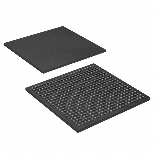
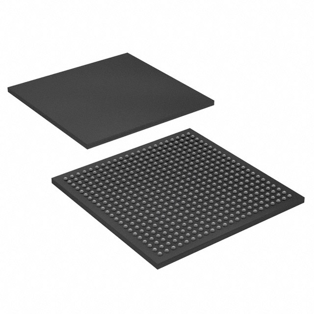
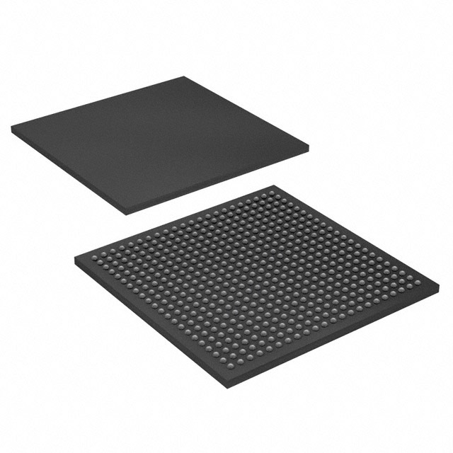
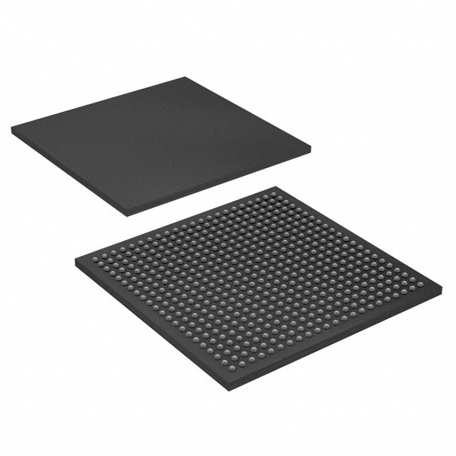
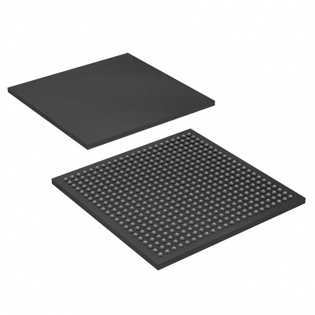
Cyclone® II Field Programmable Gate Array (FPGA) IC 294 594432 50528 484-BGA |
|---|---|
| Quantity | 1,032 Available (as of October 7, 2026) |
| Product Category | Field Programmable Gate Array (FPGA) |
|---|---|
| Manufacturer | Intel |
| Manufacturing Status | Active |
| Manufacturer Standard Lead Time | 26 Weeks |
| Datasheet |
Specifications & Environmental
| Device Package | 484-FBGA (23x23) | Grade | Commercial | Operating Temperature | 0°C – 85°C | ||
|---|---|---|---|---|---|---|---|
| Package / Case | 484-BGA | Number of I/O | 294 | Voltage | 1.15 V - 1.25 V | ||
| Mounting Method | Surface Mount | RoHS Compliance | RoHS non-compliant | REACH Compliance | REACH Unaffected | ||
| Moisture Sensitivity Level | 3 (168 Hours) | Number of LABs/CLBs | 3158 | Number of Logic Elements/Cells | 50528 | ||
| Number of Gates | N/A | ECCN | 3A991D | HTS Code | 8542.39.0001 | ||
| Qualification | N/A | Total RAM Bits | 594432 |
Overview of EP2C50F484C6 – Cyclone® II Field Programmable Gate Array (FPGA) IC 294 594432 50528 484-BGA
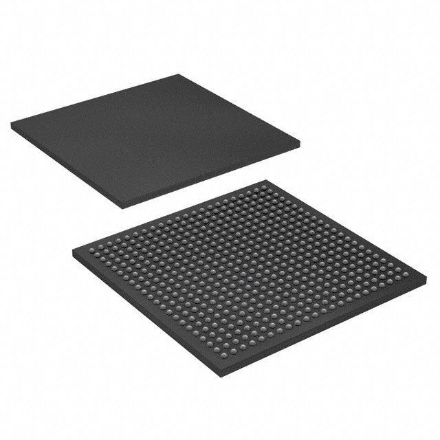
The EP2C50F484C6 is a Cyclone II family FPGA providing a balance of programmable logic, embedded memory and flexible I/O for commercial applications. It integrates 50,528 logic elements and approximately 0.59 Mbits of embedded memory in a compact 484‑FBGA (23×23) surface‑mount package.
Designed for low-cost embedded processing and DSP-oriented designs, this Cyclone II device supports on‑chip resources such as embedded multipliers, PLLs and a global clock network, plus configuration and test features documented in the Cyclone II device handbook.
Key Features
- Logic Capacity — 50,528 logic elements provide a substantial programmable fabric for combinational and sequential logic implementation.
- Embedded Memory — Approximately 0.59 Mbits of on‑chip RAM for buffering, FIFO and local data storage requirements.
- I/O Resources — 294 user I/O pins to support broad interfacing needs and external memory connections.
- Configurable Clocking — On‑chip PLLs and a global clock network support a range of clock distribution and timing architectures as described in the device handbook.
- DSP and Multiplier Support — Embedded multipliers and dedicated routing enable digital signal processing functions within the Cyclone II architecture.
- Configuration & Test — JTAG boundary‑scan support and documented configuration schemes facilitate device programming and production testing.
- Package & Mounting — 484‑FBGA (23×23) surface‑mount package for high‑density board integration.
- Power Supply — Operates from a 1.15 V to 1.25 V core supply range.
- Commercial Temperature Range — Rated for operation from 0 °C to 85 °C.
- RoHS Compliant — Conforms to RoHS environmental requirements.
Typical Applications
- Embedded Processing — Low‑cost embedded processing solutions that require on‑chip logic and memory for control and data handling tasks.
- Digital Signal Processing — DSP‑oriented implementations leveraging embedded multipliers and dedicated routing for arithmetic and filtering functions.
- External Memory Interface — Designs requiring flexible external memory interfacing supported by abundant I/O and documented external memory interface options.
- Prototyping & Custom Logic — Rapid development of custom digital circuits, leveraging programmable logic, configuration options and boundary‑scan testing.
Unique Advantages
- Substantial On‑chip Logic and Memory: 50,528 logic elements combined with approximately 0.59 Mbits of embedded RAM reduce the need for external logic and memory in many designs.
- Flexible I/O Count: 294 user I/Os enable broad peripheral and external memory interfacing without immediate need for additional I/O expanders.
- Configurable Clocking & DSP Support: Integrated PLLs, a documented global clock network and embedded multipliers simplify clocking strategies and DSP implementations.
- Production‑Ready Testability: JTAG boundary‑scan and comprehensive configuration options support streamlined production testing and in‑system programming.
- Compact, High‑Density Package: 484‑FBGA (23×23) footprint allows dense board layouts while maintaining surface‑mount assembly compatibility.
- Documented Family Support: Cyclone II device handbook provides architecture, timing and application guidance to accelerate design and verification.
Why Choose EP2C50F484C6?
The EP2C50F484C6 positions itself as a commercial‑grade Cyclone II FPGA that combines a large programmable fabric with embedded memory and extensive I/O in a compact BGA package. Its documented architecture—covering logic array blocks, embedded memory, PLLs, multipliers and configuration features—supports designs focused on embedded processing and DSP functions.
This device is suited to designers who need a well‑documented FPGA family for scalable prototypes and production systems operating in commercial temperature ranges, offering predictable integration of logic, memory and I/O with established device handbook support.
Request a quote or submit a product inquiry to receive pricing and availability information for EP2C50F484C6.





















Date Founded: 1968
Headquarters: Santa Clara, California, USA
Employees: 130,000+
Revenue: $54.23 Billion
Certifications and Memberships: ISO9001:2015, ISO14001:2015, ISO17025:2017, ISO27001:2022, ISO45001:2018, ISO50001:2018


