
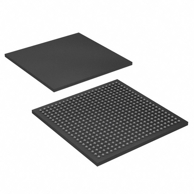
EP2C50F484C8
| Part Description |
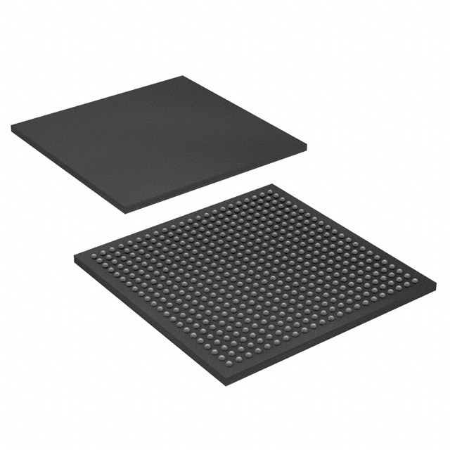
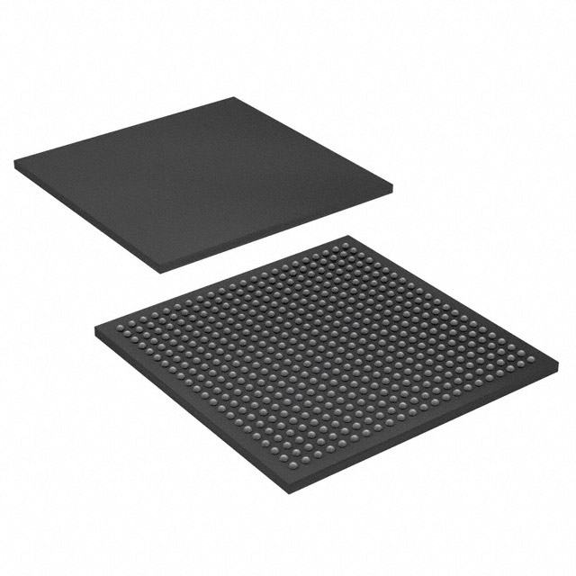
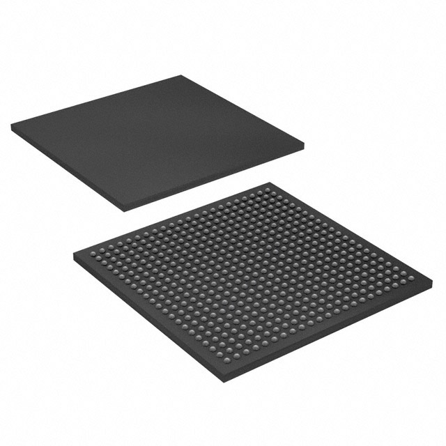
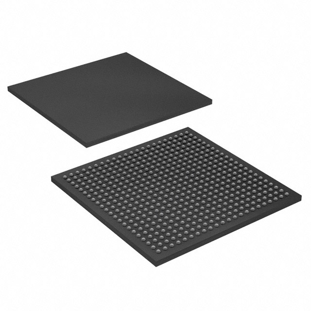
Cyclone® II Field Programmable Gate Array (FPGA) IC 294 594432 50528 484-BGA |
|---|---|
| Quantity | 878 Available (as of October 7, 2026) |
| Product Category | Field Programmable Gate Array (FPGA) |
|---|---|
| Manufacturer | Intel |
| Manufacturing Status | Active |
| Manufacturer Standard Lead Time | 26 Weeks |
| Datasheet |
Specifications & Environmental
| Device Package | 484-FBGA (23x23) | Grade | Commercial | Operating Temperature | 0°C – 85°C | ||
|---|---|---|---|---|---|---|---|
| Package / Case | 484-BGA | Number of I/O | 294 | Voltage | 1.15 V - 1.25 V | ||
| Mounting Method | Surface Mount | RoHS Compliance | RoHS non-compliant | REACH Compliance | REACH Unaffected | ||
| Moisture Sensitivity Level | 3 (168 Hours) | Number of LABs/CLBs | 3158 | Number of Logic Elements/Cells | 50528 | ||
| Number of Gates | N/A | ECCN | 3A991D | HTS Code | 8542.39.0001 | ||
| Qualification | N/A | Total RAM Bits | 594432 |
Overview of EP2C50F484C8 – Cyclone® II FPGA, 50,528 Logic Elements, 484‑BGA
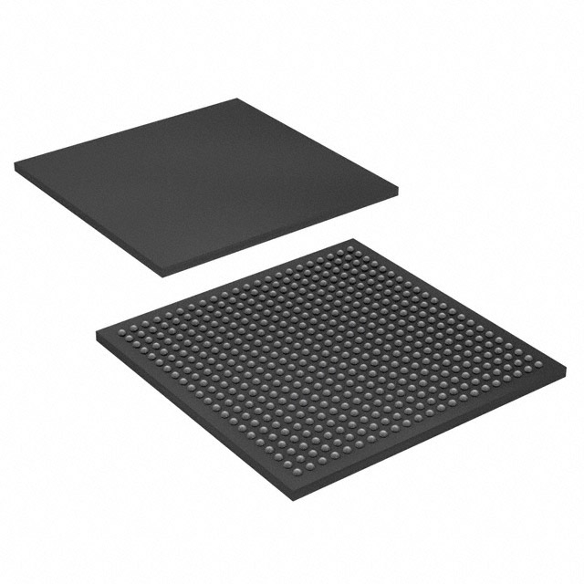
The EP2C50F484C8 is a Cyclone® II field‑programmable gate array (FPGA) in a 484‑ball BGA package designed for commercial embedded and DSP applications. It integrates 50,528 logic elements, substantial on‑chip memory, and a large I/O count to support complex logic, memory interfacing, and high‑speed I/O functions within a compact surface‑mount package.
Built on the Cyclone II architecture, this device targets low‑cost embedded processing and DSP use cases while providing documented architecture features such as a global clock network, PLLs, embedded multipliers, and M4K embedded memory blocks.
Key Features
- Core Capacity 50,528 logic elements for implementing complex state machines, control logic, and custom datapaths.
- Embedded Memory Approximately 0.57 Mbits of on‑chip RAM (594,432 bits) organized with M4K memory blocks as described in the Cyclone II device handbook.
- I/O Density and Flexibility 294 I/O pins to support broad interface requirements; the Cyclone II architecture includes support for advanced I/O standards and high‑speed differential interfaces.
- Clocking and Timing Global clock network and integrated PLLs provide flexible clock distribution and phase‑locked loop functionality for timing and clock management.
- Embedded DSP Resources Dedicated embedded multipliers for accelerating arithmetic and signal‑processing operations as described in the device handbook.
- Configuration & Test IEEE 1149.1 (JTAG) boundary‑scan support and multiple configuration schemes documented for programming and in‑system test.
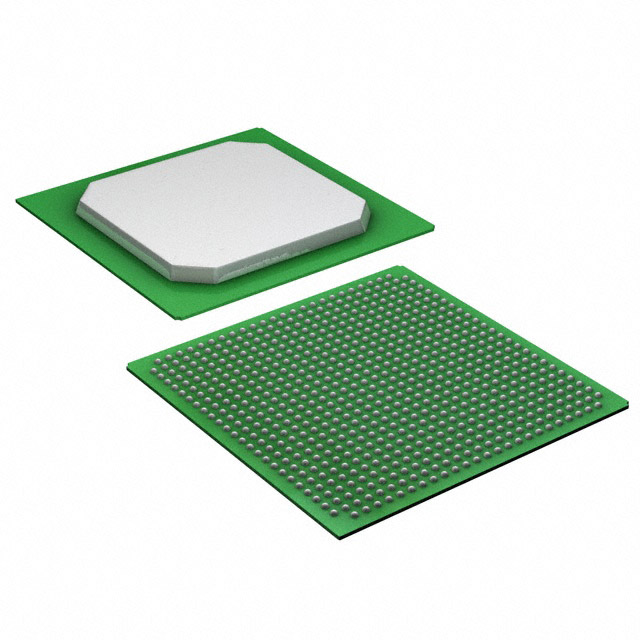
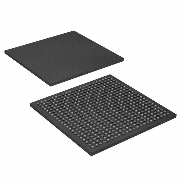
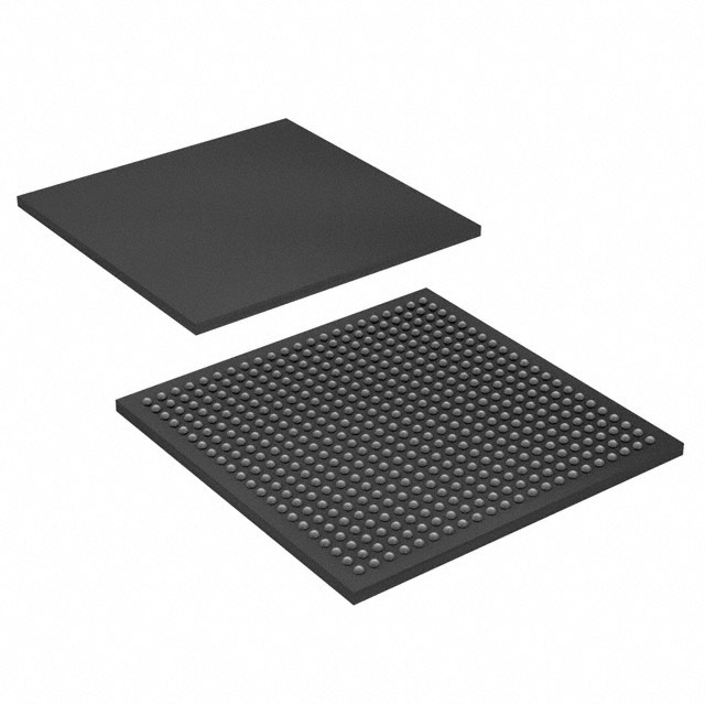
- Package & Mounting 484‑FBGA (23×23) surface‑mount package (484‑BGA) for compact board integration.
- Power and Operating Range Core supply voltage range 1.15 V to 1.25 V; commercial operating temperature range 0 °C to 85 °C.
- Environmental Compliance RoHS compliant.
Typical Applications
- Embedded Processing Implement low‑cost embedded controllers and custom processing cores using the Cyclone II architecture and significant logic capacity.
- DSP and Signal Processing Use embedded multipliers and on‑chip memory to implement filters, arithmetic pipelines, and other DSP functions.
- High‑Density I/O and Memory Interfaces Leverage 294 I/Os and Cyclone II external memory interfacing features for board‑level bridging, bus control, and memory controllers.
- Custom Logic and Control Deploy the device for complex state machines, protocol bridging, and application‑specific accelerators that require combined logic, memory, and I/O.
Unique Advantages
- Significant Logic Capacity: 50,528 logic elements enable implementation of large custom designs without external glue logic.
- Integrated Memory and DSP Resources: Approximately 0.57 Mbits of embedded RAM plus embedded multipliers support memory‑intensive and arithmetic workloads on‑chip.
- High I/O Count: 294 I/Os provide flexibility for multiple parallel interfaces, external memory buses, and mixed‑signal board designs.
- Documented Architecture: Features such as the global clock network, PLLs, M4K memory blocks, and configuration options are detailed in the Cyclone II device handbook for design planning and implementation.
- Compact BGA Package: 484‑FBGA (23×23) surface‑mount package reduces PCB footprint while maintaining routing density for complex designs.
- Commercial Grade and Compliance: Designed for commercial temperature ranges (0 °C to 85 °C) and RoHS compliant for regulatory alignment.
Why Choose EP2C50F484C8?
The EP2C50F484C8 delivers a balanced combination of logic capacity, on‑chip memory, DSP resources, and a high I/O count in a compact 484‑BGA package. It is well suited for designers implementing low‑cost embedded processing and DSP solutions where documented Cyclone II architecture features—such as global clocking, PLLs, M4K memory blocks, and embedded multipliers—are required.
Supported by the Cyclone II device handbook documentation, this commercial‑grade FPGA is appropriate for projects that need measurable logic density, configurable clocking, and broad interface capability while conforming to RoHS requirements.
Request a quote or submit an inquiry to get pricing and availability for the EP2C50F484C8 FPGA.





















Date Founded: 1968
Headquarters: Santa Clara, California, USA
Employees: 130,000+
Revenue: $54.23 Billion
Certifications and Memberships: ISO9001:2015, ISO14001:2015, ISO17025:2017, ISO27001:2022, ISO45001:2018, ISO50001:2018


