
EP2C50F672C6
| Part Description |
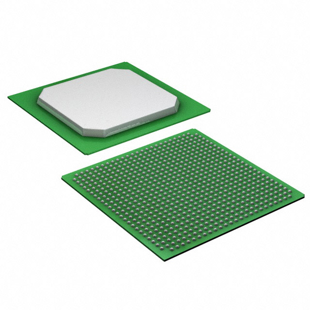
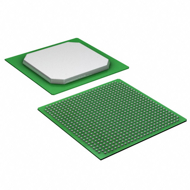
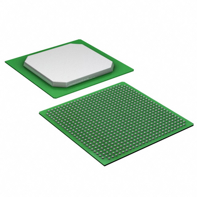
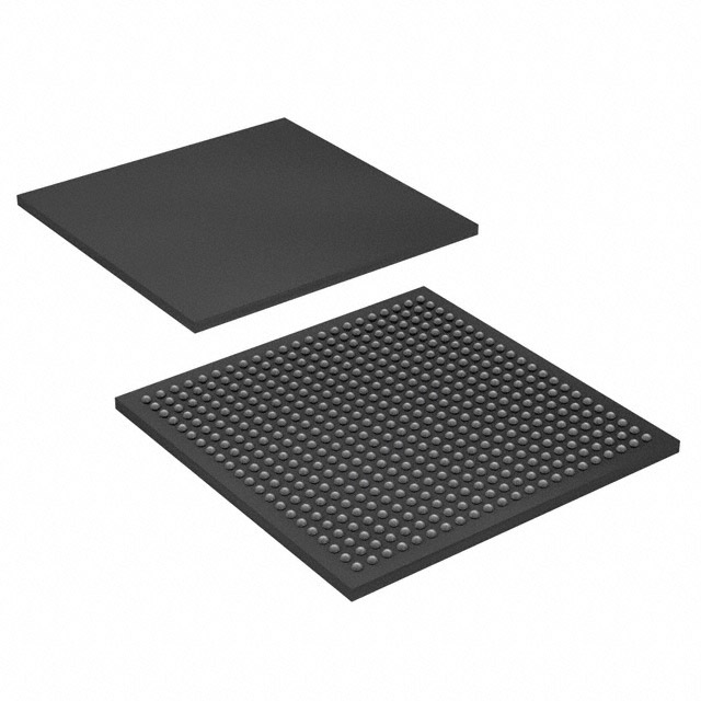
Cyclone® II Field Programmable Gate Array (FPGA) IC 450 594432 50528 672-BGA |
|---|---|
| Quantity | 600 Available (as of October 8, 2026) |
| Product Category | Field Programmable Gate Array (FPGA) |
|---|---|
| Manufacturer | Intel |
| Manufacturing Status | Active |
| Manufacturer Standard Lead Time | 26 Weeks |
| Datasheet |
Specifications & Environmental
| Device Package | 672-FBGA (27x27) | Grade | Commercial | Operating Temperature | 0°C – 85°C | ||
|---|---|---|---|---|---|---|---|
| Package / Case | 672-BGA | Number of I/O | 450 | Voltage | 1.15 V - 1.25 V | ||
| Mounting Method | Surface Mount | RoHS Compliance | RoHS non-compliant | REACH Compliance | REACH Unaffected | ||
| Moisture Sensitivity Level | 3 (168 Hours) | Number of LABs/CLBs | 3158 | Number of Logic Elements/Cells | 50528 | ||
| Number of Gates | N/A | ECCN | 3A991D | HTS Code | 8542.39.0001 | ||
| Qualification | N/A | Total RAM Bits | 594432 |
Overview of EP2C50F672C6 – Cyclone® II FPGA, 50,528 Logic Elements, 672‑BGA
The EP2C50F672C6 is an Intel Cyclone® II field programmable gate array (FPGA) offering 50,528 logic elements in a high‑density 672‑ball BGA package. Built around the Cyclone II architecture, this device targets low‑cost embedded processing and DSP-oriented designs that require substantial logic capacity, on‑chip memory, and flexible I/O.
Key on‑chip resources include approximately 0.59 Mbits of embedded memory and dedicated architectural features such as embedded multipliers, PLLs and a global clock network as described in the Cyclone II device handbook. The device is supplied for commercial applications with a 1.15 V to 1.25 V core voltage range and an operating temperature range of 0 °C to 85 °C.
Key Features
- Core Capacity 50,528 logic elements provide the programmable fabric needed to implement complex control, glue logic, and custom processing functions.
- Embedded Memory Approximately 0.59 Mbits of on‑chip RAM (594,432 bits) supports local buffering, FIFOs and small data stores for deterministic processing.
- DSP Resources & Clocking Architecture includes embedded multipliers and PLLs along with a global clock network to support synchronous logic and low‑cost DSP solutions described in the Cyclone II handbook.
- I/O Density and Flexibility 450 user I/O pins with Cyclone II I/O features such as programmable drive strength, programmable pull‑ups, series on‑chip termination, and support for differential interfaces and multiple I/O standards.
- Power Core supply range of 1.15 V to 1.25 V allows design integration with modern system rails; power characteristics and timing parameters are documented in the device handbook.
- Package & Mounting 672‑FBGA (27 × 27) package in a surface‑mount form factor provides a compact, high‑pin‑count solution for board layouts requiring dense logic and I/O.
- Operating Range & Grade Commercial grade device rated for 0 °C to 85 °C operation and RoHS compliant.
Typical Applications
- Embedded processing — Implements control engines, protocol handling and glue logic where substantial programmable logic and on‑chip RAM keep latency low and eliminate external components.
- Low‑cost DSP solutions — Uses embedded multipliers, memory and PLLs for signal processing tasks in cost‑sensitive applications.
- External memory interfacing — Cyclone II I/O structure and dedicated routing support external memory interface designs and board‑level memory controllers.
- High‑density I/O bridging — 450 I/Os allow the device to act as a bridge or aggregator between multiple peripherals and system buses, leveraging programmable I/O features for signal integrity.
Unique Advantages
- Substantial programmable capacity: 50,528 logic elements enable implementation of complex logic functions on a single device, reducing BOM and board area.
- On‑chip memory for deterministic behavior: Approximately 0.59 Mbits of embedded RAM provides local buffering and state storage that reduces dependence on external memory for many designs.
- Integrated DSP and clock infrastructure: Embedded multipliers, PLLs and a documented global clock network support synchronous DSP and timing‑sensitive designs without extensive external timing components.
- High I/O count with advanced I/O features: 450 I/Os and programmable drive/termination options simplify high‑speed interfacing and multi‑standard connectivity on complex boards.
- Compact production package: 672‑FBGA (27×27) surface‑mount package provides high pin‑count in a compact footprint for space‑constrained designs.
- Documented platform: The Cyclone II family is supported by a comprehensive device handbook that details architecture, timing, I/O and configuration options for engineering reference.
Why Choose EP2C50F672C6?
The EP2C50F672C6 balances significant programmable logic capacity with on‑chip memory and DSP resources in a compact 672‑BGA package, making it suitable for engineers designing low‑cost embedded processing and DSP systems. Its combination of 50,528 logic elements, approximately 0.59 Mbits of embedded RAM, and 450 I/Os provides an integrated platform that can reduce external components and simplify board design.
This commercial‑grade Cyclone II device is a practical choice for designs that require documented architecture, flexible I/O configuration, and predictable operating conditions (1.15 V–1.25 V core, 0 °C–85 °C). Engineers can rely on the Cyclone II handbook for detailed implementation guidance and electrical/timing specifications.
Request a quote or submit an inquiry to obtain pricing, lead‑time and availability for the EP2C50F672C6. Our team can provide the procurement details and support needed to evaluate this Cyclone II FPGA for your project requirements.





















Date Founded: 1968
Headquarters: Santa Clara, California, USA
Employees: 130,000+
Revenue: $54.23 Billion
Certifications and Memberships: ISO9001:2015, ISO14001:2015, ISO17025:2017, ISO27001:2022, ISO45001:2018, ISO50001:2018


