
EP2C50F484I8
| Part Description |
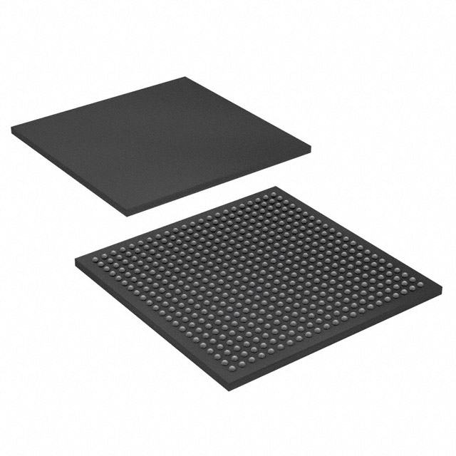
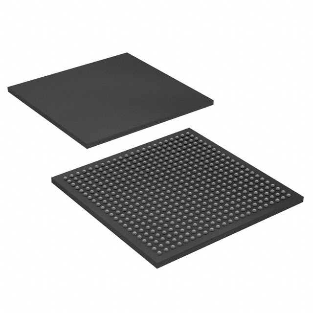
Cyclone® II Field Programmable Gate Array (FPGA) IC 294 594432 50528 484-BGA |
|---|---|
| Quantity | 1,075 Available (as of October 7, 2026) |
| Product Category | Field Programmable Gate Array (FPGA) |
|---|---|
| Manufacturer | Intel |
| Manufacturing Status | Active |
| Manufacturer Standard Lead Time | 26 Weeks |
| Datasheet |
Specifications & Environmental
| Device Package | 484-FBGA (23x23) | Grade | Industrial | Operating Temperature | -40°C – 100°C | ||
|---|---|---|---|---|---|---|---|
| Package / Case | 484-BGA | Number of I/O | 294 | Voltage | 1.15 V - 1.25 V | ||
| Mounting Method | Surface Mount | RoHS Compliance | RoHS non-compliant | REACH Compliance | REACH Unaffected | ||
| Moisture Sensitivity Level | 3 (168 Hours) | Number of LABs/CLBs | 3158 | Number of Logic Elements/Cells | 50528 | ||
| Number of Gates | N/A | ECCN | 3A991D | HTS Code | 8542.39.0001 | ||
| Qualification | N/A | Total RAM Bits | 594432 |
Overview of EP2C50F484I8 – Cyclone® II Field Programmable Gate Array (FPGA) IC 294 594432 50528 484-BGA
The EP2C50F484I8 is an Intel Cyclone® II FPGA delivering 50,528 logic elements in a compact 484-BGA package. Built on the Cyclone II architecture, the device combines sizable on-chip memory and DSP-friendly resources with a broad I/O complement for embedded, industrial, and communications applications.
Key capabilities include approximately 0.59 Mbits of embedded memory, support for advanced I/O features and high-speed differential interfaces, integrated clocking (including PLL support), and an industrial operating range from −40 °C to 100 °C. The device operates from a core supply of 1.15 V to 1.25 V and is RoHS compliant.
Key Features
- Core Logic 50,528 logic elements delivered by the Cyclone II architecture for mid-density programmable logic implementations.
- Embedded Memory Approximately 0.59 Mbits of on-chip RAM, with M4K memory blocks and flexible memory modes for buffering, FIFOs, and local storage.
- DSP & Arithmetic Resources Integrated embedded multipliers and multiplier routing support suitable for arithmetic and signal-processing functions described in the Cyclone II handbook.
- Clocking and Timing Global clock network and Phase-Locked Loop (PLL) capability to support multiple clock domains and on-chip clock distribution.
- I/O Structure & Features 294 general-purpose I/O pins with support for programmable drive strength, slew-rate control, bus-hold, programmable pull-ups, series on‑chip termination, and high‑speed differential interfaces.
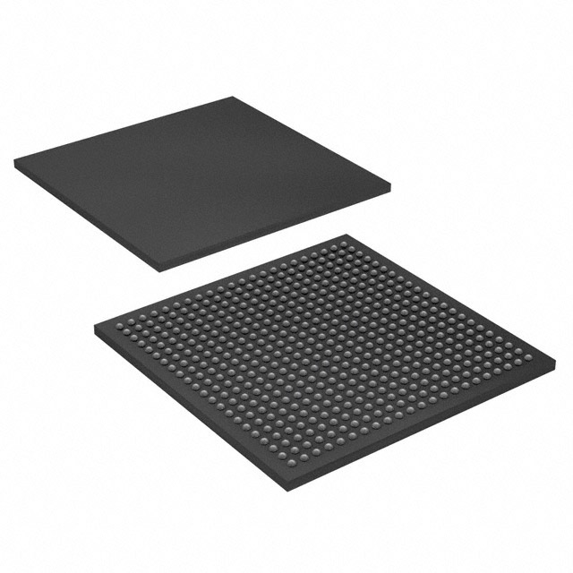
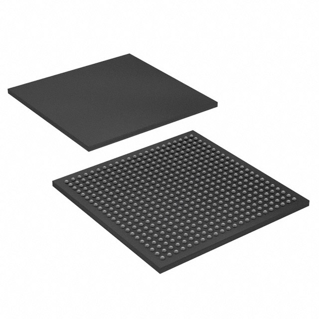
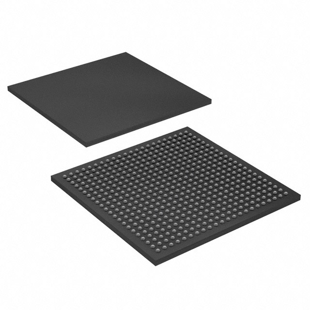
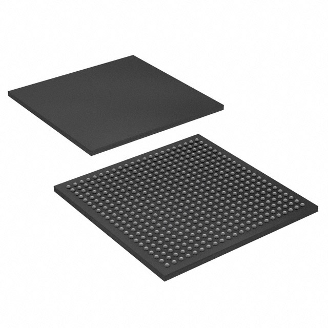
- Package & Mounting 484‑BGA package (supplier package: 484‑FBGA, 23×23) in a surface-mount form factor for compact board-level integration.
- Power & Environmental Core supply voltage range 1.15 V–1.25 V and industrial operating temperature range of −40 °C to 100 °C; RoHS compliant.
Typical Applications
- Industrial Control Implement motor control, PLC logic, and machine-interface functions using the device’s sizable logic and I/O resources alongside industrial temperature ratings.
- Embedded Signal Processing Use embedded multipliers and on-chip RAM for fixed-point DSP tasks, filtering, and data buffering in compact FPGA-based accelerators.
- Communications Interfaces Leverage high-speed differential I/O and flexible I/O standards to implement protocol bridging, SERDES-lite interfaces, and custom transceiver logic.
- Custom Embedded Systems Create glue logic, bus bridging, and control subsystems that require abundant I/O and moderate logic capacity in a single package.
Unique Advantages
- High logic capacity: 50,528 logic elements enable complex state machines, control logic, and moderate-density custom datapaths without external ASICs.
- Integrated memory and DSP support: Approximately 0.59 Mbits of embedded RAM plus embedded multipliers simplify implementation of buffering and arithmetic functions on chip.
- Flexible, high-density I/O: 294 I/O pins with programmable drive, terminations, and differential support reduces external components and eases interface design.
- Robust clocking options: Global clock networks and PLLs in the Cyclone II family support multi-domain clocking and synchronized system timing.
- Industrial-ready operation: −40 °C to 100 °C operating range and RoHS compliance support deployment in industrial environments.
- Compact BGA package: 484‑FBGA (23×23) surface-mount package minimizes PCB area while providing substantial I/O and logic resources.
Why Choose EP2C50F484I8?
The EP2C50F484I8 positions itself as a mid-density Cyclone II FPGA choice for designers needing a balanced combination of logic capacity, embedded memory, DSP resources, and flexible I/O in a compact 484‑BGA footprint. Its documented Cyclone II architecture features — including M4K memory blocks, embedded multipliers, PLLs, and advanced I/O controls — make it suitable for embedded systems, industrial control, and communications designs that require on-chip integration and reliable operation across an industrial temperature range.
Supported by the Cyclone II device handbook and datasheet documentation, the EP2C50F484I8 is appropriate for teams seeking a well-documented, programmable silicon option with verifiable electrical and environmental specifications for production designs.
Request a quote or submit an inquiry to receive pricing and availability information for the EP2C50F484I8. Our team can assist with ordering details and providing the device’s datasheet and supporting documentation upon request.





















Date Founded: 1968
Headquarters: Santa Clara, California, USA
Employees: 130,000+
Revenue: $54.23 Billion
Certifications and Memberships: ISO9001:2015, ISO14001:2015, ISO17025:2017, ISO27001:2022, ISO45001:2018, ISO50001:2018


