
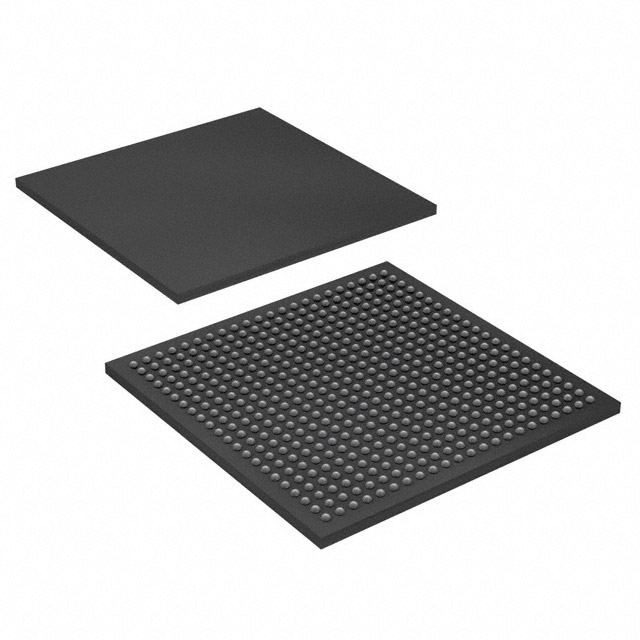
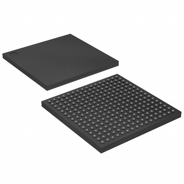
EP2C5F256C6
| Part Description |
Cyclone® II Field Programmable Gate Array (FPGA) IC 158 119808 4608 256-LBGA |
|---|---|
| Quantity | 511 Available (as of June 15, 2026) |

| Product Category | Field Programmable Gate Array (FPGA) |
|---|---|
| Manufacturer | Intel |
| Manufacturing Status | Active |
| Manufacturer Standard Lead Time | 26 Weeks |
| Datasheet |
Specifications & Environmental
| Device Package | 256-FBGA (17x17) | Grade | Commercial | Operating Temperature | 0°C – 85°C | ||
|---|---|---|---|---|---|---|---|
| Package / Case | 256-LBGA | Number of I/O | 158 | Voltage | 1.15 V - 1.25 V | ||
| Mounting Method | Surface Mount | RoHS Compliance | RoHS non-compliant | REACH Compliance | REACH Unaffected | ||
| Moisture Sensitivity Level | 3 (168 Hours) | Number of LABs/CLBs | 288 | Number of Logic Elements/Cells | 4608 | ||
| Number of Gates | N/A | ECCN | 3A991D | HTS Code | 8542.39.0001 | ||
| Qualification | N/A | Total RAM Bits | 119808 |
Overview of EP2C5F256C6 – Cyclone® II FPGA, 4608 logic elements
The EP2C5F256C6 is a Cyclone® II Field Programmable Gate Array (FPGA) IC from Intel, offered in a 256-LBGA package. It implements the Cyclone II architecture and provides a balanced mix of logic capacity, on-chip memory, and rich I/O suited to cost-sensitive embedded and DSP-focused designs.
Documented in the Cyclone II Device Handbook, this device targets low-cost embedded processing and DSP solutions where a defined number of logic elements, abundant I/O, and a standard commercial temperature range are required.
Key Features
- Core Logic 4,608 logic elements for implementing combinational and sequential logic functions.
- Embedded Memory Approximately 0.12 Mbits (119,808 bits) of on-chip RAM for buffering, FIFOs, and small data stores.
- I/O Capacity 158 user I/O pins to support multiple peripheral interfaces and parallel connections.
- Package & Mounting 256-LBGA package (supplier device package: 256-FBGA, 17×17) with surface-mount mounting for PCB assembly.
- Power Core supply range of 1.15 V to 1.25 V for integration with standard FPGA power rails.
- Temperature & Grade Commercial grade operation from 0 °C to 85 °C.
- Family Architecture Highlights The Cyclone II family handbook documents architecture elements such as global clock networks, PLLs, embedded multipliers, I/O features, and programmable memory modes that apply to Cyclone II devices.
- Regulatory RoHS compliant.
Typical Applications
- Low‑Cost Embedded Processing Ideal for cost-sensitive embedded control and processing tasks that require programmable logic and on-chip memory.
- Low‑Cost DSP Solutions Suitable for signal-processing blocks where a combination of logic elements and on-chip RAM is required, as referenced in the Cyclone II documentation.
- Interface Bridging & Glue Logic 158 I/Os enable the device to serve as an interface hub between multiple parallel and serial peripherals.
Unique Advantages
- Compact logic capacity: 4,608 logic elements deliver a predictable development target for mid-range FPGA designs.
- On‑chip memory for local data storage: ~0.12 Mbits of RAM reduces the need for external memory in many buffering and control tasks.
- High I/O count: 158 user I/Os support diverse peripheral and bus connectivity without immediate external glue logic.
- Standard commercial temperature grade: 0 °C to 85 °C simplifies selection for mainstream consumer and industrial-adjacent applications that do not require extended-temperature parts.
- Surface-mount 256-LBGA packaging: Compact board footprint with a supplier-specified 256-FBGA (17×17) outline for consistent assembly and layout planning.
- RoHS compliance: Conforms to common environmental requirements for lead-free manufacturing.
Why Choose EP2C5F256C6?
The EP2C5F256C6 positions itself as a Cyclone II family device that balances logic capacity, embedded memory, and abundant I/O in a compact 256-LBGA footprint. Its documented Cyclone II architecture features—summarized in the Cyclone II Device Handbook—support common embedded and DSP design building blocks such as clocking, memory modes, and multiplier resources.
This device is well suited to designers and procurement teams building low-cost embedded processing, interface bridging, or DSP-lean systems that require a defined logic density, substantial I/O, and standard commercial operating conditions. Its combination of measurable specifications and family-level architecture documentation supports predictable system integration and lifecycle planning.
Request a quote or submit your requirements to receive pricing and availability for the EP2C5F256C6. Our team can provide lead-time details and support for volume inquiries.


Date Founded: 1968
Headquarters: Santa Clara, California, USA
Employees: 130,000+
Revenue: $54.23 Billion
Certifications and Memberships: ISO9001:2015, ISO14001:2015, ISO17025:2017, ISO27001:2022, ISO45001:2018, ISO50001:2018


