
EP2C5F256C6N
| Part Description |
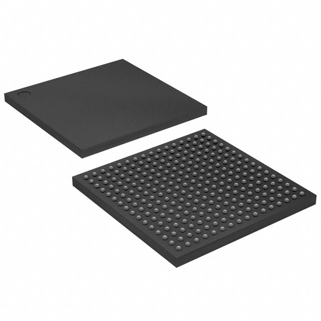
Cyclone® II Field Programmable Gate Array (FPGA) IC 158 119808 4608 256-LBGA |
|---|---|
| Quantity | 1,021 Available (as of June 15, 2026) |

| Product Category | Field Programmable Gate Array (FPGA) |
|---|---|
| Manufacturer | Intel |
| Manufacturing Status | Not For New Designs |
| Manufacturer Standard Lead Time | 26 Weeks |
| Datasheet |
Specifications & Environmental
| Device Package | 256-FBGA (17x17) | Grade | Commercial | Operating Temperature | 0°C – 85°C | ||
|---|---|---|---|---|---|---|---|
| Package / Case | 256-LBGA | Number of I/O | 158 | Voltage | 1.15 V - 1.25 V | ||
| Mounting Method | Surface Mount | RoHS Compliance | RoHS Compliant | REACH Compliance | REACH Unaffected | ||
| Moisture Sensitivity Level | 3 (168 Hours) | Number of LABs/CLBs | 288 | Number of Logic Elements/Cells | 4608 | ||
| Number of Gates | N/A | ECCN | 3A991D | HTS Code | 8542.39.0001 | ||
| Qualification | N/A | Total RAM Bits | 119808 |
Overview of EP2C5F256C6N – Cyclone® II Field Programmable Gate Array (FPGA) IC 158 119808 4608 256-LBGA
The EP2C5F256C6N is a Cyclone II family FPGA optimized for low-cost embedded processing and DSP-oriented designs. It integrates 288 logic array blocks and 4,608 logic elements with on-chip memory and dedicated routing and clock resources to support a wide range of system functions.
Designed for commercial applications, this surface-mount device comes in a 256-LBGA (256-FBGA, 17×17) package, offers 158 user I/O pins, and operates from a 1.15 V to 1.25 V core supply within a 0 °C to 85 °C temperature range.
Key Features
- Core Logic — 288 logic array blocks (LABs) providing a total of 4,608 logic elements for implementing custom digital logic, control, and glue functions.
- Embedded Memory — 119,808 bits of on-chip RAM (approximately 0.12 Mbits) for buffering, state storage, and small on-chip data structures; includes M4K memory routing support referenced in the device handbook.
- DSP Resources — Integrated embedded multipliers and multiplier routing interfaces to support arithmetic and signal-processing functions described in the Cyclone II device documentation.
- Clocking and PLLs — Global clock network and phase-locked loop (PLL) resources for flexible clock distribution and frequency control across the device.
- I/O and Interface Support — 158 I/O pins with advanced I/O standard support, high-speed differential interface capability, programmable drive strength, on-chip series termination, and other I/O features documented for Cyclone II devices.
- Power and Operating Range — Core voltage supply range of 1.15 V to 1.25 V and commercial operating temperature range of 0 °C to 85 °C.
- Package and Mounting — Surface-mount 256-LBGA package (supplier package: 256-FBGA, 17×17) for compact board integration.
- Compliance — RoHS compliant for environmental and manufacturing process compatibility.
Typical Applications
- Low-Cost Embedded Processing — Implement control logic, protocol handling, and custom peripherals where a compact, reconfigurable logic device is required.
- DSP and Signal Processing — Use embedded multipliers and on-chip RAM for filtering, transform, and fixed-point arithmetic tasks in cost-sensitive DSP applications.
- Interface and Glue Logic — Provide protocol conversion, bus bridging, and timing adaptation using the device’s flexible I/O and global clock resources.
- Prototyping and Educational Systems — Leverage the Cyclone II architecture and logic capacity for prototyping digital designs and teaching FPGA concepts in lab environments.
Unique Advantages
- Configurable Logic Capacity: 4,608 logic elements across 288 LABs deliver a balanced resource set for mid-size control and processing tasks.
- Embedded Memory Efficiency: Approximately 0.12 Mbits of on-chip RAM reduces external memory dependence for small buffers and state machines.
- DSP-Ready Resources: Integrated multipliers and routing support enable common signal-processing functions without adding external accelerators.
- Flexible Clocking: Global clock networks and PLLs provide precise clock distribution and frequency synthesis for synchronous designs.
- Versatile I/O: 158 I/O pins with support for advanced standards and on-chip termination simplify high-speed interface implementation.
- Compact, Surface-Mount Package: 256-LBGA (256-FBGA, 17×17) offers a small PCB footprint for space-constrained designs.
Why Choose EP2C5F256C6N?
The EP2C5F256C6N delivers a practical combination of configurable logic, on-chip memory, DSP-oriented resources, and flexible I/O in a compact 256-LBGA package. Its Cyclone II architecture provides the routing, clocking, and peripheral features described in the device handbook, making it suitable for cost-sensitive embedded and DSP applications that require reprogrammable logic and moderate resource capacity.
This commercial-grade FPGA is a good fit for engineers and system designers seeking a balanced, reconfigurable building block for control, interface, and signal-processing tasks, backed by documentation and family-level features in the Cyclone II device handbook.
Request a quote or submit an inquiry for pricing and availability for the EP2C5F256C6N to begin integrating this Cyclone II FPGA into your next design.


Date Founded: 1968
Headquarters: Santa Clara, California, USA
Employees: 130,000+
Revenue: $54.23 Billion
Certifications and Memberships: ISO9001:2015, ISO14001:2015, ISO17025:2017, ISO27001:2022, ISO45001:2018, ISO50001:2018


