
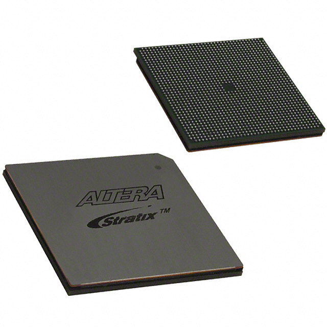
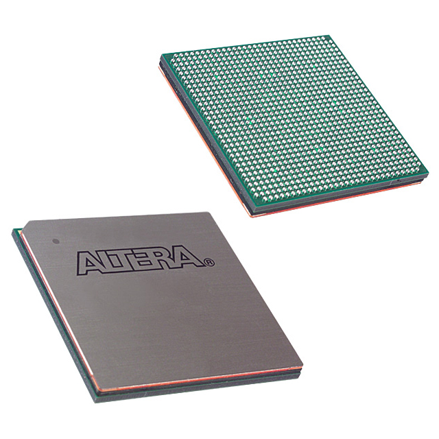
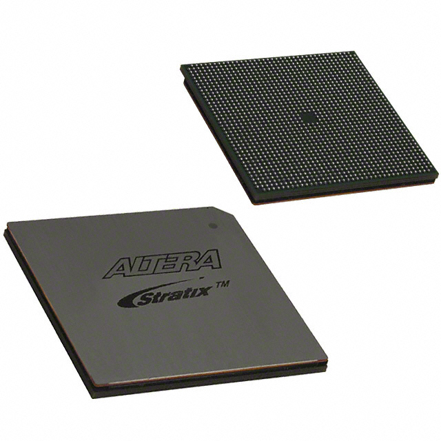
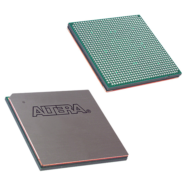
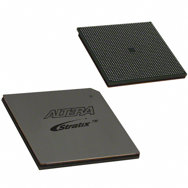
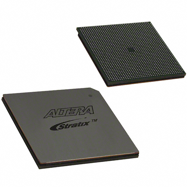
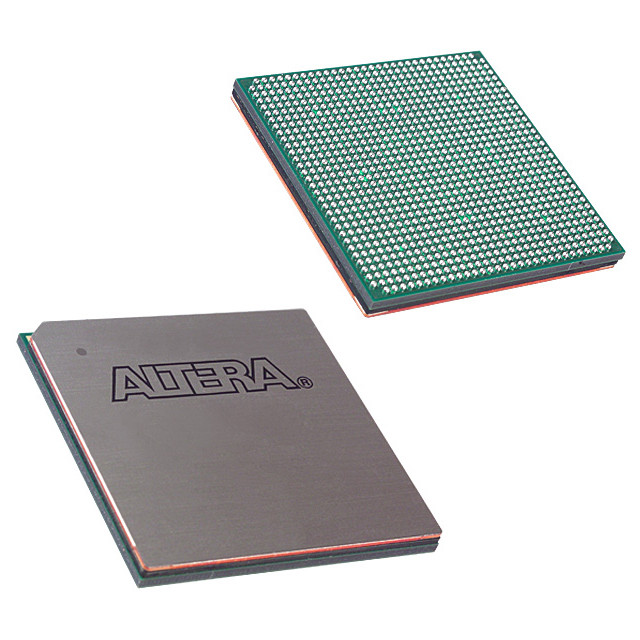
EP2S130F1508C3
| Part Description |
Stratix® II Field Programmable Gate Array (FPGA) IC 1126 6747840 132540 1508-BBGA, FCBGA |
|---|---|
| Quantity | 316 Available (as of October 8, 2026) |
| Product Category | Field Programmable Gate Array (FPGA) |
|---|---|
| Manufacturer | Intel |
| Manufacturing Status | Obsolete |
| Manufacturer Standard Lead Time | Contact Us |
| Datasheet |
Specifications & Environmental
| Device Package | 1508-FBGA, FC (40x40) | Grade | Commercial | Operating Temperature | 0°C – 85°C | ||
|---|---|---|---|---|---|---|---|
| Package / Case | 1508-BBGA, FCBGA | Number of I/O | 1126 | Voltage | 1.15 V - 1.25 V | ||
| Mounting Method | Surface Mount | RoHS Compliance | RoHS non-compliant | REACH Compliance | REACH Unaffected | ||
| Moisture Sensitivity Level | 3 (168 Hours) | Number of LABs/CLBs | 6627 | Number of Logic Elements/Cells | 132540 | ||
| Number of Gates | N/A | ECCN | 3A001A7A | HTS Code | 8542.39.0001 | ||
| Qualification | N/A | Total RAM Bits | 6747840 |
Overview of EP2S130F1508C3 – Stratix® II Field Programmable Gate Array (FPGA) IC, 1508-BBGA
The EP2S130F1508C3 is a Stratix® II family FPGA providing a large logic fabric and extensive I/O integration in a 1508-BBGA (40 × 40 FCBGA) surface-mount package. It combines 132,540 logic elements with approximately 6.75 Mbits of embedded RAM and 1,126 I/O pins to support complex, high‑density programmable designs.
Designed for applications that require substantial on-chip logic, significant embedded memory, and flexible I/O, this device leverages the Stratix II architecture—documented in the device handbook—for features such as PLLs, multi‑track interconnect, DSP blocks, and advanced I/O capabilities.
Key Features
- Logic Capacity 132,540 logic elements (cells) provide large programmable fabric for complex state machines, control logic, and custom datapaths.
- Embedded Memory Approximately 6.75 Mbits of on‑chip RAM (total RAM bits: 6,747,840) for buffering, frame storage, and on‑chip data structures.
- I/O Density & Flexibility 1,126 I/O pins and on‑chip support for a wide range of I/O standards as described in the Stratix II device handbook, enabling diverse interface implementations.
- Signal Processing & Clocking Architecture includes DSP block capabilities and integrated PLL/clock networks (as documented) to support synchronous designs and DSP workloads.
- Power Supply Supports core voltage supply in the range 1.15 V to 1.25 V to match Stratix II device requirements.
- Package & Mounting 1508‑FBGA (1508‑BBGA, FCBGA, 40 × 40) surface‑mount package for high I/O count and compact board integration.
- Operating Conditions Commercial grade operation from 0 °C to 85 °C, and RoHS compliant.
Typical Applications
- External memory interfacing Implement memory controllers and high‑bandwidth interfaces using the device’s on‑chip clocking and I/O resources.
- Digital signal processing Use integrated DSP block features and large logic capacity for signal filtering, transforms, and custom compute pipelines.
- High‑pin‑count custom I/O Implement complex multi‑lane or multi‑standard interfaces utilizing up to 1,126 I/O pins and documented I/O standard support.
- System integration and prototyping Leverage substantial programmable resources and embedded memory for board‑level prototyping and system validation.
Unique Advantages
- Large programmable fabric: 132,540 logic elements enable complex logic integration that reduces the need for multiple discrete devices.
- Substantial on‑chip memory: Approximately 6.75 Mbits of embedded RAM supports buffering, packet storage, and algorithm state without external memory.
- Extensive I/O count: 1,126 I/O pins provide flexibility for multi‑lane interfaces, dense connector I/O, and parallel peripherals.
- Advanced architecture features: Stratix II device handbook documents DSP blocks, PLLs, and hierarchical clocking to simplify timing and performance design choices.
- Compact, high‑density package: 1508‑FBGA (40 × 40) surface‑mount package balances I/O density with board footprint considerations.
- Commercial temperature and compliance: Operates from 0 °C to 85 °C and is RoHS compliant for standard commercial product environments.
Why Choose EP2S130F1508C3?
The EP2S130F1508C3 positions itself as a high‑capacity FPGA solution within the Stratix II family, delivering a combination of large logic element count, significant embedded RAM, and broad I/O resources in a compact FCBGA package. Its documented architecture—covering DSP resources, PLLs, and advanced I/O support—makes it suitable for designs that require integrated signal processing, complex interfacing, and substantial on‑chip storage.
This device is well suited for engineering teams developing prototypes or production systems that need a scalable, programmable platform with strong vendor‑documented architecture and features. The part’s electrical and thermal specifications, along with RoHS compliance, provide a clear basis for system design and long‑term integration in commercial environments.
Request a quote or submit an order inquiry to check availability, lead time, and pricing for EP2S130F1508C3.





















Date Founded: 1968
Headquarters: Santa Clara, California, USA
Employees: 130,000+
Revenue: $54.23 Billion
Certifications and Memberships: ISO9001:2015, ISO14001:2015, ISO17025:2017, ISO27001:2022, ISO45001:2018, ISO50001:2018


