
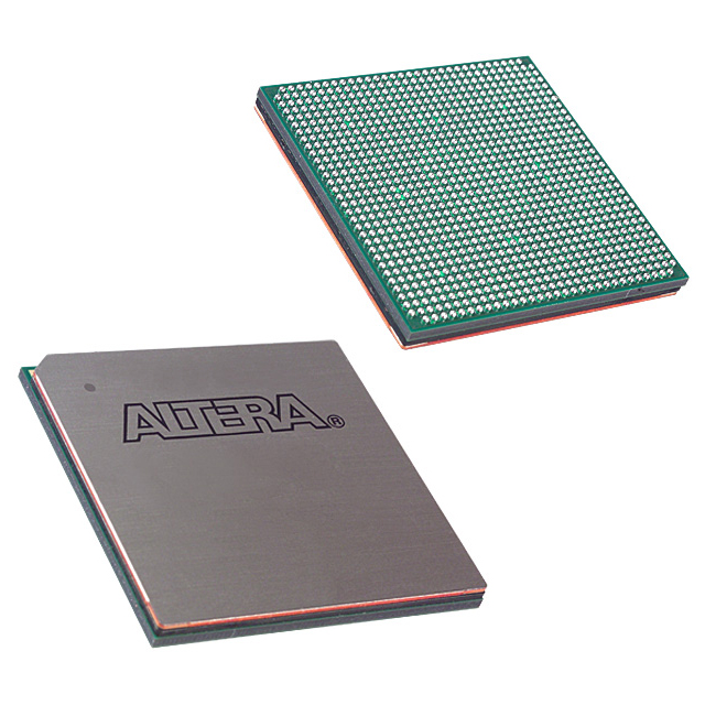
EP2S130F1508C3N
| Part Description |
Stratix® II Field Programmable Gate Array (FPGA) IC 1126 6747840 132540 1508-BBGA, FCBGA |
|---|---|
| Quantity | 153 Available (as of June 18, 2026) |

| Product Category | Field Programmable Gate Array (FPGA) |
|---|---|
| Manufacturer | Intel |
| Manufacturing Status | Obsolete |
| Manufacturer Standard Lead Time | Contact Us |
| Datasheet |
Specifications & Environmental
| Device Package | 1508-FBGA, FC (40x40) | Grade | Commercial | Operating Temperature | 0°C – 85°C | ||
|---|---|---|---|---|---|---|---|
| Package / Case | 1508-BBGA, FCBGA | Number of I/O | 1126 | Voltage | 1.15 V - 1.25 V | ||
| Mounting Method | Surface Mount | RoHS Compliance | RoHS Compliant | REACH Compliance | REACH Unaffected | ||
| Moisture Sensitivity Level | 3 (168 Hours) | Number of LABs/CLBs | 6627 | Number of Logic Elements/Cells | 132540 | ||
| Number of Gates | N/A | ECCN | 3A001A7A | HTS Code | 8542.39.0001 | ||
| Qualification | N/A | Total RAM Bits | 6747840 |
Overview of EP2S130F1508C3N – Stratix® II Field Programmable Gate Array, 1508-BBGA FCBGA
The EP2S130F1508C3N is a Stratix® II FPGA IC from Intel designed for commercial-grade system designs requiring high logic density and extensive I/O. This device integrates 132,540 logic elements across 6,627 logic array blocks and approximately 6.75 Mbits of embedded RAM, enabling large, on-chip digital systems and buffering.
With 1,126 user I/Os, a 1508-BBGA FCBGA package (supplier package: 1508-FBGA, FC 40×40), and a core supply range of 1.15 V to 1.25 V, the EP2S130F1508C3N targets high-pin-count applications where integration density, on-chip memory, and configurable logic resources are primary requirements. The device is RoHS compliant and rated for commercial operation from 0 °C to 85 °C.
Key Features
- High Logic Capacity 132,540 logic elements arranged across 6,627 logic array blocks to implement complex digital designs and dense logic fabrics.
- Embedded Memory Approximately 6.75 Mbits of on-chip RAM for data buffering, FIFOs, and local storage to support large state machines and memory-mapped functions.
- Extensive I/O 1,126 user I/O pins suitable for designs requiring large external connectivity and parallel interfaces.
- Power and Operating Range Core supply voltage from 1.15 V to 1.25 V; commercial operating temperature range of 0 °C to 85 °C.
- Package and Mounting 1508-BBGA, FCBGA package (supplier device package: 1508-FBGA, FC 40×40) with surface-mount mounting type for compact board-level integration.
- Standards and Compliance RoHS compliant to meet lead-free and environmental requirements for commercial electronic products.
Typical Applications
- High-density digital processing Use the large logic element count and abundant on-chip RAM to implement complex state machines, protocol stacks, and custom compute pipelines.
- Memory interfacing and buffering Embedded RAM and extensive I/O enable local buffering and external memory interfacing in systems that require large temporary storage.
- Multi-I/O control systems 1,126 I/Os support designs with numerous parallel interfaces, signal aggregation, or large connector pinouts.
- Prototyping and system integration Commercial temperature-rated FPGA suitable for development platforms and integration into production electronics where commercial-grade operation is required.
Unique Advantages
- Large on-chip logic density: 132,540 logic elements provide the headroom needed to implement multi-function systems on a single FPGA, reducing external FPGA count and system complexity.
- Significant embedded memory: Approximately 6.75 Mbits of RAM allows for substantial local data storage, minimizing bandwidth requirements to external memory in many designs.
- Very high I/O count: 1,126 I/Os enable broad external connectivity and facilitate parallel interfaces, sensor arrays, and wide datapath implementations.
- Compact, surface-mount package: 1508-BBGA/1508-FBGA (40×40) packaging supports dense PCB layouts while maintaining the pin count required for complex systems.
- Commercial temperature and RoHS compliance: Rated 0 °C to 85 °C and RoHS compliant for commercial electronics production and regulatory requirements.
Why Choose EP2S130F1508C3N?
The EP2S130F1508C3N delivers a balance of high logic capacity, substantial on-chip memory, and a very large I/O complement in a compact FCBGA package — a combination well suited to commercial systems that demand integration and flexibility. Its specification set makes it appropriate for designers building complex digital processing, high-bandwidth buffering, or multi-interface control systems.
Selected for projects that require scalable logic resources and extensive connectivity, this Stratix II FPGA supports integration-driven designs and long-term platform development where vendor documentation and device family support are part of the design lifecycle.
Request a quote or submit a pricing inquiry for EP2S130F1508C3N to begin integrating this Stratix® II FPGA into your next commercial design.


Date Founded: 1968
Headquarters: Santa Clara, California, USA
Employees: 130,000+
Revenue: $54.23 Billion
Certifications and Memberships: ISO9001:2015, ISO14001:2015, ISO17025:2017, ISO27001:2022, ISO45001:2018, ISO50001:2018


