
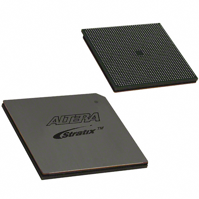
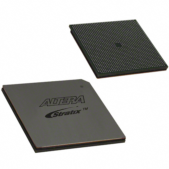
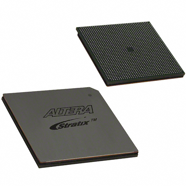
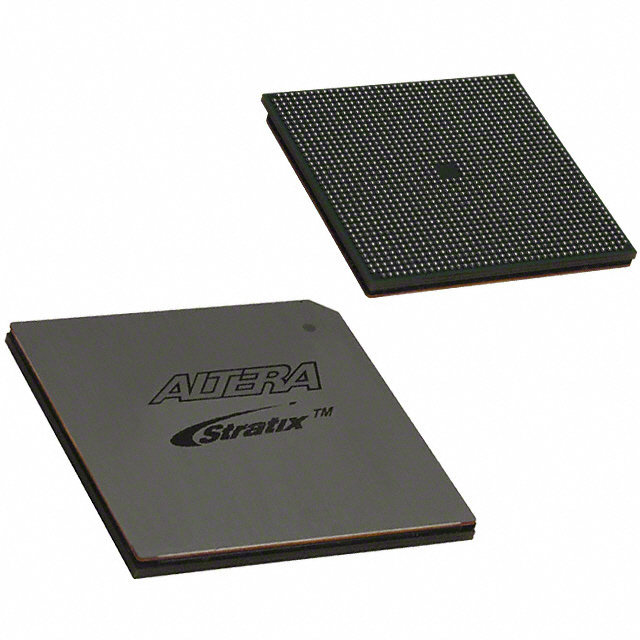
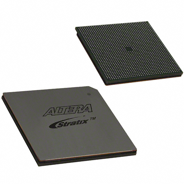
EP2S130F1508I4
| Part Description |
Stratix® II Field Programmable Gate Array (FPGA) IC 1126 6747840 132540 1508-BBGA, FCBGA |
|---|---|
| Quantity | 727 Available (as of October 8, 2026) |
| Product Category | Field Programmable Gate Array (FPGA) |
|---|---|
| Manufacturer | Intel |
| Manufacturing Status | Obsolete |
| Manufacturer Standard Lead Time | Contact Us |
| Datasheet |
Specifications & Environmental
| Device Package | 1508-FBGA, FC (40x40) | Grade | Industrial | Operating Temperature | -40°C – 100°C | ||
|---|---|---|---|---|---|---|---|
| Package / Case | 1508-BBGA, FCBGA | Number of I/O | 1126 | Voltage | 1.15 V - 1.25 V | ||
| Mounting Method | Surface Mount | RoHS Compliance | RoHS non-compliant | REACH Compliance | REACH Unaffected | ||
| Moisture Sensitivity Level | 3 (168 Hours) | Number of LABs/CLBs | 6627 | Number of Logic Elements/Cells | 132540 | ||
| Number of Gates | N/A | ECCN | 3A001A7A | HTS Code | 8542.39.0001 | ||
| Qualification | N/A | Total RAM Bits | 6747840 |
Overview of EP2S130F1508I4 – Stratix® II FPGA — 132,540 logic elements, 1508‑BBGA
The EP2S130F1508I4 is a Stratix® II Field Programmable Gate Array (FPGA) in a 1508‑BBGA (FCBGA) package. It integrates a high-density logic fabric with embedded memory and a large I/O complement to support complex, custom digital designs.
Documented architecture elements in the Stratix II handbook include Logic Array Blocks (LABs), Adaptive Logic Modules, DSP blocks, PLLs and extensive I/O features, providing a platform for designs that require substantial logic resources, on-chip memory, and high I/O counts.
Key Features
- Logic Capacity — 6,627 LABs and 132,540 logic elements provide significant resources for complex FPGA designs.
- Embedded Memory — Approximately 6.7 Mbits of on‑chip RAM to support buffering, FIFOs, and local data storage for processing pipelines.
- I/O Density — 1,126 I/O pins to accommodate wide external interfaces and multi‑bus connectivity.
- Clocking & DSP — Datasheet content documents dedicated DSP blocks and multiple PLL/clock network options for synchronized, high‑throughput designs.
- Configuration & Debugging — Supports JTAG boundary‑scan, SignalTap II embedded logic analyzer, and multiple configuration schemes as described in the device handbook.
- Power Supply Range — Core supply specified from 1.15 V to 1.25 V for defined power domain planning.
- Temperature & Grade — Industrial grade device with an operating range of −40 °C to 100 °C for deployment in demanding environments.
- Package & Mounting — 1508‑BBGA (FCBGA, supplier package listed as 1508‑FBGA, 40×40) with surface‑mount mounting for compact board integration.
- Standards & Compliance — RoHS compliant.
Typical Applications
- High‑Performance Signal Processing — On‑chip DSP blocks and approximately 6.7 Mbits of embedded memory support filtering, transforms, and other streaming signal tasks.
- Custom I/O and Protocol Bridging — 1,126 I/Os allow implementation of wide parallel interfaces, multi‑channel data capture, and protocol translation.
- Memory Interface and Controller Logic — Documented external memory interfacing and abundant logic/memory resources enable custom memory controllers and buffering solutions.
Unique Advantages
- High logic density: 132,540 logic elements and 6,627 LABs provide headroom for complex, multi‑module designs without immediate migration.
- Substantial embedded memory: Approximately 6.7 Mbits of on‑chip RAM reduces the need for external memory in many buffering and streaming applications.
- Very large I/O count: 1,126 I/Os let you bring numerous external signals onto the FPGA for dense board‑level integration.
- Industrial temperature rating: −40 °C to 100 °C operation supports deployment in industrial and temperature‑challenging environments.
- Flexible configuration and debug: Built‑in support for JTAG, SignalTap II, and multiple configuration schemes documented in the Stratix II handbook eases bring‑up and validation.
- Robust package options: 1508‑BBGA (FCBGA) surface‑mount package provides a compact, soldered solution for production assemblies.
Why Choose EP2S130F1508I4?
The EP2S130F1508I4 combines a high logic element count, substantial embedded RAM, and a very large I/O complement in an industrial‑rated Stratix II FPGA package. Its documented architecture—including LABs, Adaptive Logic Modules, DSP blocks, and advanced clocking—provides a solid foundation for complex digital designs that require integrated processing, memory, and connectivity.
This device is suited to engineering teams building systems that need significant on‑chip resources and robust environmental operation. The Stratix II handbook details the configuration, debugging, and I/O capabilities that help accelerate development and validation.
Request a quote or submit a procurement inquiry to get pricing and availability for the EP2S130F1508I4. Include your required quantity and delivery timeline for a prompt response.





















Date Founded: 1968
Headquarters: Santa Clara, California, USA
Employees: 130,000+
Revenue: $54.23 Billion
Certifications and Memberships: ISO9001:2015, ISO14001:2015, ISO17025:2017, ISO27001:2022, ISO45001:2018, ISO50001:2018


