
EP2S15F672C4
| Part Description |
Stratix® II Field Programmable Gate Array (FPGA) IC 366 419328 15600 672-BBGA |
|---|---|
| Quantity | 1,349 Available (as of June 15, 2026) |

| Product Category | Field Programmable Gate Array (FPGA) |
|---|---|
| Manufacturer | Intel |
| Manufacturing Status | Obsolete |
| Manufacturer Standard Lead Time | Contact Us |
| Datasheet |
Specifications & Environmental
| Device Package | 672-FBGA (27x27) | Grade | Commercial | Operating Temperature | 0°C – 85°C | ||
|---|---|---|---|---|---|---|---|
| Package / Case | 672-BBGA | Number of I/O | 366 | Voltage | 1.15 V - 1.25 V | ||
| Mounting Method | Surface Mount | RoHS Compliance | RoHS non-compliant | REACH Compliance | REACH Unaffected | ||
| Moisture Sensitivity Level | 3 (168 Hours) | Number of LABs/CLBs | 780 | Number of Logic Elements/Cells | 15600 | ||
| Number of Gates | N/A | ECCN | 3A991D | HTS Code | 8542.39.0001 | ||
| Qualification | N/A | Total RAM Bits | 419328 |
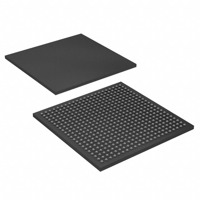
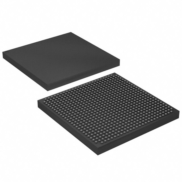
Overview of EP2S15F672C4 – Stratix® II FPGA, 672‑BBGA
The EP2S15F672C4 is a Stratix® II Field Programmable Gate Array (FPGA) in a 672‑ball BGA package. It implements the Stratix II device architecture and provides a balance of logic capacity, on‑chip memory and high I/O count for complex digital and signal processing designs.
Device documentation for the Stratix II family highlights on‑chip DSP resources, PLLs, high‑speed I/O options and configurable memory architectures, making this device suitable for designs that require integrated clocking, embedded memory and flexible I/O connectivity.
Key Features
- Logic Capacity — 15,600 logic elements to implement combinational and sequential logic functions.
- Embedded Memory — Approximately 0.42 Mbits of on‑chip RAM (419,328 bits) for buffering, FIFOs and small data stores.
- I/O Density — 366 user I/O pins to support wide parallel buses and multiple external interfaces.
- Package & Mounting — 672‑BBGA surface‑mount package; supplier package listed as 672‑FBGA (27×27) for compact board integration.
- Power — Core voltage range 1.15 V to 1.25 V to match Stratix II power domains and board power budgets.
- Operating Range — Commercial grade operation from 0 °C to 85 °C.
- Architecture Enhancements — Stratix II architecture includes DSP blocks, PLLs and TriMatrix memory concepts as described in the device handbook, supporting clock management and signal processing implementations.
- Configuration & Debug — Family documentation references JTAG boundary‑scan support and embedded logic analysis features for configuration and debugging workflows.
- Environmental — RoHS compliant.
Typical Applications
- High‑performance digital systems — Use the device’s 15,600 logic elements and large I/O count for complex control and data‑path implementations.
- Signal processing and communications — On‑chip DSP resources, embedded memory and PLLs support applications requiring deterministic data flow and clock management.
- Memory interface and bridging — Ample I/O and embedded RAM allow interfacing to external memories and buffering for bus conversion or protocol bridging.
- Embedded prototyping and system integration — The 672‑ball BGA package and comprehensive Stratix II documentation support board‑level prototyping and integration into multi‑board systems.
Unique Advantages
- Significant logic resources: 15,600 logic elements provide room for substantial combinatorial and sequential logic without external CPLDs.
- Compact, high‑pin package: 672‑BBGA in a 27×27 layout delivers dense I/O in a board‑space efficient footprint.
- Integrated memory: Approximately 0.42 Mbits of embedded RAM reduces external memory dependencies for on‑chip buffering and local storage.
- Precise power domain: Defined core supply range (1.15 V–1.25 V) helps with predictable power budgeting and thermal planning.
- Commercial temperature rating: Rated 0 °C to 85 °C for designs targeting commercial‑grade deployments.
- Standards‑driven documentation: Stratix II device handbook details PLLs, DSP blocks, I/O structures and configuration options to streamline development and verification.
Why Choose EP2S15F672C4?
The EP2S15F672C4 combines a sizeable logic fabric with embedded memory and a high I/O count in a compact 672‑ball BGA package, making it a practical choice for designers who need substantial on‑chip resources and flexible interfacing in a commercial‑grade device. Its Stratix II architecture provides documented primitives for DSP, clock management and advanced I/O to support complex digital and signal processing implementations.
This part is suitable for engineering teams building systems that require dense logic, integrated memory and comprehensive architecture documentation to accelerate development and verification. The device’s RoHS compliance and clear electrical and thermal parameters support predictable integration into production designs.
Request a quote or submit a procurement inquiry to evaluate EP2S15F672C4 for your next FPGA design.


Date Founded: 1968
Headquarters: Santa Clara, California, USA
Employees: 130,000+
Revenue: $54.23 Billion
Certifications and Memberships: ISO9001:2015, ISO14001:2015, ISO17025:2017, ISO27001:2022, ISO45001:2018, ISO50001:2018


