
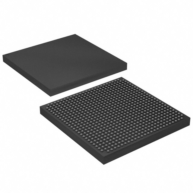
EP2S15F672C5N
| Part Description |
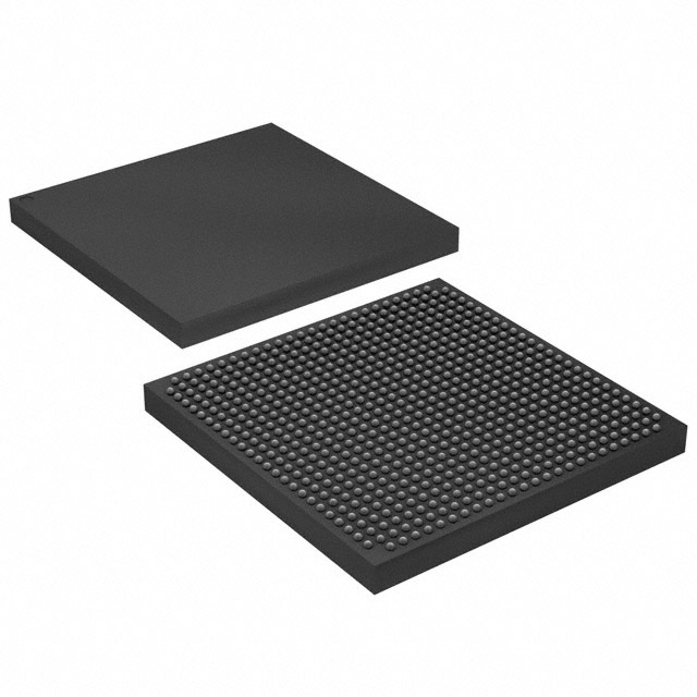
Stratix® II Field Programmable Gate Array (FPGA) IC 366 419328 15600 672-BBGA |
|---|---|
| Quantity | 330 Available (as of October 7, 2026) |
| Product Category | Field Programmable Gate Array (FPGA) |
|---|---|
| Manufacturer | Intel |
| Manufacturing Status | Obsolete |
| Manufacturer Standard Lead Time | Contact Us |
| Datasheet |
Specifications & Environmental
| Device Package | 672-FBGA (27x27) | Grade | Commercial | Operating Temperature | 0°C – 85°C | ||
|---|---|---|---|---|---|---|---|
| Package / Case | 672-BBGA | Number of I/O | 366 | Voltage | 1.15 V - 1.25 V | ||
| Mounting Method | Surface Mount | RoHS Compliance | RoHS Compliant | REACH Compliance | REACH Unaffected | ||
| Moisture Sensitivity Level | 3 (168 Hours) | Number of LABs/CLBs | 780 | Number of Logic Elements/Cells | 15600 | ||
| Number of Gates | N/A | ECCN | 3A991D | HTS Code | 8542.39.0001 | ||
| Qualification | N/A | Total RAM Bits | 419328 |
Overview of EP2S15F672C5N – Stratix® II FPGA, 15,600 logic elements, 672‑BBGA
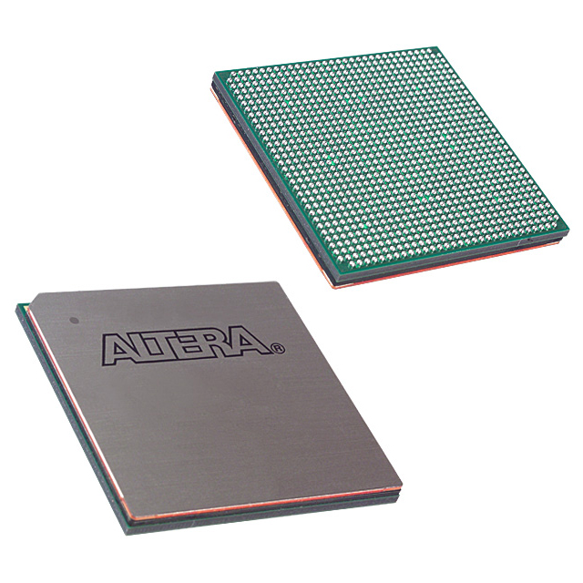
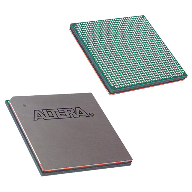
The EP2S15F672C5N is a Stratix® II Field Programmable Gate Array (FPGA) IC from Intel, delivered in a 672‑ball BGA package. It provides a high-density programmable logic resource with integrated on‑chip memory and a large I/O count suitable for compact, board‑level FPGA designs.
Architected for FPGA applications that require significant logic capacity, embedded RAM and flexible I/O, this device targets commercial designs operating within standard temperature and supply ranges while conforming to RoHS requirements.
Key Features
- Programmable Logic Density 15,600 logic elements provide substantial gate-equivalent resources for complex combinational and sequential logic implementation.
- Embedded Memory Approximately 0.42 Mbits (419,328 bits) of on‑chip RAM for FIFOs, buffers, and small data stores integrated with the logic fabric.
- High I/O Count 366 I/O pins enable dense external interfacing for parallel buses, memory interfaces, and mixed-signal connectivity.
- Power Supply Core supply range of 1.15 V to 1.25 V to match system power rails and ensure predictable core operation.
- Commercial Temperature Grade Rated for operation from 0 °C to 85 °C for standard commercial applications.
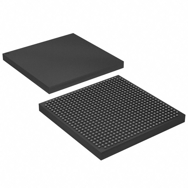
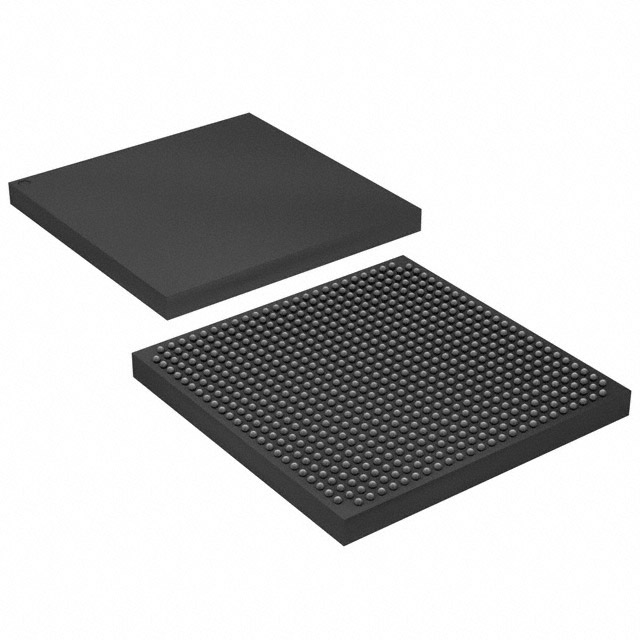
- Package & Mounting 672‑BBGA package (supplier package listed as 672‑FBGA, 27×27) with surface‑mount mounting for compact PCB integration.
- Standards & Compliance RoHS‑compliant for environmental conformity in commercial production.
- Stratix II Family Architecture (Series Features) The Stratix II device family architecture includes advanced elements such as PLLs and clock networks, dedicated DSP blocks, TriMatrix memory organization, comprehensive I/O structure (including DDR support), and configuration/testing capabilities like JTAG and an embedded logic analyzer, as documented in the Stratix II device handbook.
Typical Applications
- FPGA‑based Prototyping Use as a programmable platform for validating digital designs and implementing prototype hardware where substantial logic and memory resources are required.
- High‑density Logic Integration Consolidate glue logic, state machines, and custom peripherals into a single device using the device’s 15,600 logic elements and embedded RAM.
- Memory and Interface Bridging Implement on‑board protocol bridging and buffering leveraging the device’s embedded RAM and abundant I/O for external memory and peripheral connections.
Unique Advantages
- Substantial Logic Capacity: 15,600 logic elements enable consolidation of multiple functions into a single FPGA, reducing overall BOM and board complexity.
- Integrated On‑chip Memory: Approximately 0.42 Mbits of RAM reduces dependence on external memory for small‑to‑medium sized buffering and state storage.
- Large I/O Portfolio: 366 I/Os deliver flexibility for dense external interfaces and parallel data paths without additional I/O expanders.
- Compact Surface‑Mount Package: The 672‑ball BGA (27×27 supplier package) supports high pin density in a compact footprint for space‑constrained designs.
- Family Ecosystem: Stratix II family features such as PLLs, DSP blocks, advanced clocking and configuration/testing capabilities provide architectural building blocks to accelerate system-level design.
- Commercial‑grade and RoHS‑Compliant: Designed for standard commercial environments with environmental compliance suitable for mainstream production.
Why Choose EP2S15F672C5N?
The EP2S15F672C5N balances significant programmable logic capacity, embedded memory, and high I/O density in a compact 672‑ball BGA package. Its Stratix II family architecture provides advanced clocking, DSP and memory organization features that enable complex digital functions on a single device while remaining within standard commercial operating conditions.
This part is well suited for engineers looking to integrate multiple logic functions, on‑chip buffering and extensive external interfacing in applications that operate within commercial temperature and supply ranges. Its RoHS compliance and common BGA footprint make it straightforward to incorporate into production boards.
Request a quote or submit a technical inquiry for EP2S15F672C5N to obtain pricing, availability and ordering information tailored to your project requirements.





















Date Founded: 1968
Headquarters: Santa Clara, California, USA
Employees: 130,000+
Revenue: $54.23 Billion
Certifications and Memberships: ISO9001:2015, ISO14001:2015, ISO17025:2017, ISO27001:2022, ISO45001:2018, ISO50001:2018


